Explain the term ‘doping’.
Answer
568.8k+ views
Hint: Semiconductors can be used to create devices which emanate light, can be used in electric circuits, used in photo sensors and have many other applications. There is a need to increase the conductivity of these semiconductors in order to execute these processes more efficiently. Think about what can be done in order to increase the conductivity, in order to increase the current flow.
Complete step by step answer:
A semiconductor material is a material which has conductivity in between the conductivities of the conductors and insulators, for example Silicon and Germanium. An intrinsic semiconductor is the purest form of semiconductor with no impurities. An extrinsic semiconductor is a doped semiconductor having impurities.
Doping is the process in which the intrinsic semiconductor is intentionally introduced with impurities in order to modulate its electrical and structural properties. Different techniques/methods of doping exist. The n-type semiconductor is made by doping the intrinsic semiconductor with phosphorus, arsenic, antimony, bismuth, etc. These elements are called donor impurities because it gives the semiconductor free electrons. Here, the majority carriers are electrons. The resulting material has conductivity greater than the pure semiconductor. Another type is the p-type semiconductor. The p-type semiconductor is made by doping the intrinsic semiconductor with trivalent impurity such as Boron, Aluminum, Gallium, Indium and thallium. These elements are called acceptors. These elements create a hole when surrounded with the atoms of the semiconductor. Here, the majority carriers are holes. The current flows when electrons move. In order to move, there must be holes for electrons to move in. The p-type semiconductor has more holes than electrons which allows the current to flow from hole to hole in a single direction.

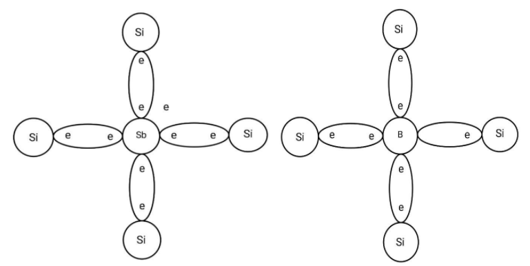
Here you can see the doped semiconductors. The left figure is for n-type where the dopant is Antimony (Sb), a pentavalent element. The right figure is for the p-type semiconductor where the dopant is Boron, a trivalent element.
Note:
In intrinsic semiconductors, the number of charge carriers depends on the properties of the material. The number of free electrons is equal to the number of holes. It is still possible that the previous statement will hold even after doping, but that will happen only if the amounts of donors and acceptors are equal.
In extrinsic semiconductor, the majority carriers can be electron or hole depending on the doping agent, thus creating two types of extrinsic semiconductors.
Complete step by step answer:
A semiconductor material is a material which has conductivity in between the conductivities of the conductors and insulators, for example Silicon and Germanium. An intrinsic semiconductor is the purest form of semiconductor with no impurities. An extrinsic semiconductor is a doped semiconductor having impurities.
Doping is the process in which the intrinsic semiconductor is intentionally introduced with impurities in order to modulate its electrical and structural properties. Different techniques/methods of doping exist. The n-type semiconductor is made by doping the intrinsic semiconductor with phosphorus, arsenic, antimony, bismuth, etc. These elements are called donor impurities because it gives the semiconductor free electrons. Here, the majority carriers are electrons. The resulting material has conductivity greater than the pure semiconductor. Another type is the p-type semiconductor. The p-type semiconductor is made by doping the intrinsic semiconductor with trivalent impurity such as Boron, Aluminum, Gallium, Indium and thallium. These elements are called acceptors. These elements create a hole when surrounded with the atoms of the semiconductor. Here, the majority carriers are holes. The current flows when electrons move. In order to move, there must be holes for electrons to move in. The p-type semiconductor has more holes than electrons which allows the current to flow from hole to hole in a single direction.

Here you can see the doped semiconductors. The left figure is for n-type where the dopant is Antimony (Sb), a pentavalent element. The right figure is for the p-type semiconductor where the dopant is Boron, a trivalent element.
Note:
In intrinsic semiconductors, the number of charge carriers depends on the properties of the material. The number of free electrons is equal to the number of holes. It is still possible that the previous statement will hold even after doping, but that will happen only if the amounts of donors and acceptors are equal.
In extrinsic semiconductor, the majority carriers can be electron or hole depending on the doping agent, thus creating two types of extrinsic semiconductors.
Recently Updated Pages
Master Class 12 Economics: Engaging Questions & Answers for Success

Master Class 12 Physics: Engaging Questions & Answers for Success

Master Class 12 English: Engaging Questions & Answers for Success

Master Class 12 Social Science: Engaging Questions & Answers for Success

Master Class 12 Maths: Engaging Questions & Answers for Success

Master Class 12 Business Studies: Engaging Questions & Answers for Success

Trending doubts
Which are the Top 10 Largest Countries of the World?

What are the major means of transport Explain each class 12 social science CBSE

Draw a labelled sketch of the human eye class 12 physics CBSE

Why cannot DNA pass through cell membranes class 12 biology CBSE

Differentiate between insitu conservation and exsitu class 12 biology CBSE

Draw a neat and well labeled diagram of TS of ovary class 12 biology CBSE


