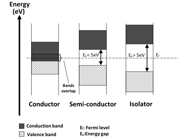
Fermi energy level for p-type extrinsic semiconductors lies:
Answer
585.6k+ views
Hint: Fermi level is used to denote the relationship between the property of the material, mainly the flow of charges to the electronic structure, to understand solid-state physics. Also, a semiconductor material has conductivity between an insulator and a metal.
Complete answer:
A semiconductor is a material whose conductivity is in between that of insulator and metals. They have holes and electrons, which contribute to their unique property. The resistivity of these materials decreases with rise in temperature. By the method called doping, the conductivity of these semiconductors can be increased.
Doping is a technique of adding impurities to the crystal; this changes the properties of the crystal.
This results in two types of semiconductors namely, the p-type and the n-type. Where p-type has more number of holes as compared to the parent semiconductor and the n-type has more number of electrons as compared to the parent semiconductor.

Here, we are talking about the p-type semiconductor, where the number of electrons is less as compared to the number of holes, and hence they are occupied by the incoming electrons. These electrons are more probable to occupy the valence bond energy than the conduction band. This creates a level called the Fermi level which is close to the valence bond.
So, the correct answer is “Option C”.
Note:
Semiconductors are materials which are made up of holes and electrons.
In the p-type semiconductor also called the acceptors, doping is done to increase the number of holes in the semiconductor; hence holes are the majority carriers. Whereas in the n-type semiconductor also called the donors, doping is done to increase the number of electrons in the semiconductor; hence electrons are the majority carriers.
Complete answer:
A semiconductor is a material whose conductivity is in between that of insulator and metals. They have holes and electrons, which contribute to their unique property. The resistivity of these materials decreases with rise in temperature. By the method called doping, the conductivity of these semiconductors can be increased.
Doping is a technique of adding impurities to the crystal; this changes the properties of the crystal.
This results in two types of semiconductors namely, the p-type and the n-type. Where p-type has more number of holes as compared to the parent semiconductor and the n-type has more number of electrons as compared to the parent semiconductor.

Here, we are talking about the p-type semiconductor, where the number of electrons is less as compared to the number of holes, and hence they are occupied by the incoming electrons. These electrons are more probable to occupy the valence bond energy than the conduction band. This creates a level called the Fermi level which is close to the valence bond.
So, the correct answer is “Option C”.
Note:
Semiconductors are materials which are made up of holes and electrons.
In the p-type semiconductor also called the acceptors, doping is done to increase the number of holes in the semiconductor; hence holes are the majority carriers. Whereas in the n-type semiconductor also called the donors, doping is done to increase the number of electrons in the semiconductor; hence electrons are the majority carriers.
Recently Updated Pages
Master Class 12 Economics: Engaging Questions & Answers for Success

Master Class 12 Physics: Engaging Questions & Answers for Success

Master Class 12 English: Engaging Questions & Answers for Success

Master Class 12 Social Science: Engaging Questions & Answers for Success

Master Class 12 Maths: Engaging Questions & Answers for Success

Master Class 12 Business Studies: Engaging Questions & Answers for Success

Trending doubts
Which are the Top 10 Largest Countries of the World?

What are the major means of transport Explain each class 12 social science CBSE

Draw a labelled sketch of the human eye class 12 physics CBSE

Why cannot DNA pass through cell membranes class 12 biology CBSE

Differentiate between insitu conservation and exsitu class 12 biology CBSE

Draw a neat and well labeled diagram of TS of ovary class 12 biology CBSE


