In forward bias, the depletion layer behaves like
A) An insulator
B) A conductor
C) A semiconductor
D) A capacitor
Answer
588.6k+ views
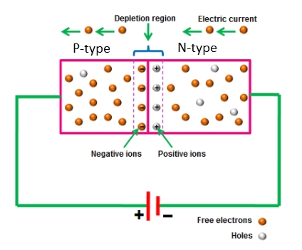
Hint: PN junction diode formed by fusing p-type semiconductor and n-type semiconductor. There is a depletion layer between the p and n-type semiconductors. That depletion layer determines the potential level for the charge carriers like electrons, holes to enter into another type. If the charge carriers from the one type can go pass the depletion layer, it can enter another type. Hence there will be a charge flow. And the conduction of current occurs in the diode.
Complete step by step answer:
(i) PN junction diode is a fusion of p and n-type semiconductors. The depletion layer determines the potential level for the charge carriers. If the depletion is wide, there will be more potential required for the charge carriers. And if the depletion layer is narrow, then the potential will be required minimum for the charge carriers.
(ii) The p-type semiconductor has more holes as its charge carriers and has few electrons. But in n-type semiconductors, there are more electrons as charge carriers and only a few holes are present in it.
(iii) If the electrons reach the holes or the holes reach the electrons, the diode conducts current. Because electrons have negative potential and holes have positive potential. But passing through the depletion layer is difficult for the electrons and holes. It needs extra potential. That potential is supplied by the external battery or any other source.

(iv) If the n-type is connected to the negative terminal (cathode), the potential for the electrons increases as it gets more negative potential. And it can pass through the depletion layer. The same goes for the p-type that is connected to the positive terminal (anode). And this process of connecting positive to positive and negative to negative is called ‘forward biasing’.
(v) While the diode is in forwarding bias, the electrons and holes can pass through the depletion layer. And the diode acts as a conductor.
When the diode is in forward bias the diode acts as a conductor. Hence, the correct option is B.
Additional information:
(i) There is another type of biasing called ‘reverse biasing’. In reverse biasing, the positive terminal is connected to n-type and the negative terminal is connected to the p-type of the semiconductor.
(ii) Reverse biasing increases the potential of the depletion layer. Hence it is very difficult for the electrons and holes to pass through it. Therefore, the diode cannot conduct current.
Note:
PN junction is known for conducting current in forward biasing. In forward bias, the depletion layer in the diode becomes thin. But in reverse bias, the depletion layer will be wider. Hence it will be difficult for the charge carriers to pass through it. But Zener diode conducts current in reverse biasing. Because it conducts current once the diode reaches the breakdown stage.
Complete step by step answer:
(i) PN junction diode is a fusion of p and n-type semiconductors. The depletion layer determines the potential level for the charge carriers. If the depletion is wide, there will be more potential required for the charge carriers. And if the depletion layer is narrow, then the potential will be required minimum for the charge carriers.
(ii) The p-type semiconductor has more holes as its charge carriers and has few electrons. But in n-type semiconductors, there are more electrons as charge carriers and only a few holes are present in it.
(iii) If the electrons reach the holes or the holes reach the electrons, the diode conducts current. Because electrons have negative potential and holes have positive potential. But passing through the depletion layer is difficult for the electrons and holes. It needs extra potential. That potential is supplied by the external battery or any other source.

(iv) If the n-type is connected to the negative terminal (cathode), the potential for the electrons increases as it gets more negative potential. And it can pass through the depletion layer. The same goes for the p-type that is connected to the positive terminal (anode). And this process of connecting positive to positive and negative to negative is called ‘forward biasing’.
(v) While the diode is in forwarding bias, the electrons and holes can pass through the depletion layer. And the diode acts as a conductor.
When the diode is in forward bias the diode acts as a conductor. Hence, the correct option is B.
Additional information:
(i) There is another type of biasing called ‘reverse biasing’. In reverse biasing, the positive terminal is connected to n-type and the negative terminal is connected to the p-type of the semiconductor.
(ii) Reverse biasing increases the potential of the depletion layer. Hence it is very difficult for the electrons and holes to pass through it. Therefore, the diode cannot conduct current.
Note:
PN junction is known for conducting current in forward biasing. In forward bias, the depletion layer in the diode becomes thin. But in reverse bias, the depletion layer will be wider. Hence it will be difficult for the charge carriers to pass through it. But Zener diode conducts current in reverse biasing. Because it conducts current once the diode reaches the breakdown stage.
Recently Updated Pages
Master Class 11 Computer Science: Engaging Questions & Answers for Success

Master Class 11 Business Studies: Engaging Questions & Answers for Success

Master Class 11 Economics: Engaging Questions & Answers for Success

Master Class 11 English: Engaging Questions & Answers for Success

Master Class 11 Maths: Engaging Questions & Answers for Success

Master Class 11 Biology: Engaging Questions & Answers for Success

Trending doubts
One Metric ton is equal to kg A 10000 B 1000 C 100 class 11 physics CBSE

There are 720 permutations of the digits 1 2 3 4 5 class 11 maths CBSE

Discuss the various forms of bacteria class 11 biology CBSE

Draw a diagram of a plant cell and label at least eight class 11 biology CBSE

State the laws of reflection of light

Explain zero factorial class 11 maths CBSE


