


The forbidden energy gap can be overcome on thermal agitation by light. The substance is
(A) An insulator
(B) A conductor
(C) A semiconductor
(D) A superconductor
Answer
233.1k+ views
Hint: In conductors and superconductors, the conduction and valence bands are overlapped, so there is already no forbidden energy gap. In insulators, the forbidden energy gap is too large to be overcome by thermal excitation. In semiconductors, the forbidden energy gap is moderate and can be overcome.
Complete step by step solution:
First of all, we need to have a clear idea of what the forbidden energy gap is.
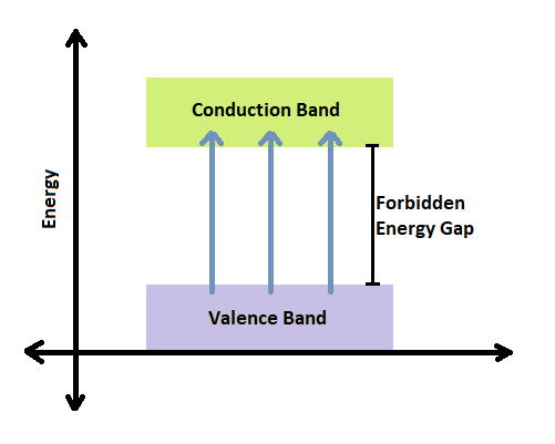
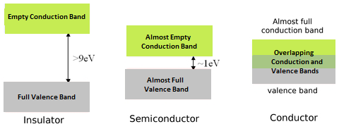
The forbidden energy band gap is the energy difference between valence band and conduction band of a substance. As the name suggests, this energy region is forbidden, that is, no electron occupies this state. This gap between valence band and conduction band, also determines the classification on the basis of electrical conductivity of a material. On the basis of electrical conductivity, materials are categorized into three main types:
Insulators: Forbidden energy gap > 9eV
Semiconductors: Forbidden energy gap ≈ 1eV
Conductors: Forbidden energy gap < 1eV
The forbidden energy band gap for all three types is shown:
Therefore, in semiconductors, the forbidden energy gap is small and can be overcome by thermal agitation, that is, by increasing temperature, unlike insulators. So, as the temperature of the semiconductor is increased, the forbidden energy gap tends to decrease.
Option (C) is correct.
Note: There is also an explicit temperature dependence of the forbidden energy gap which can be mathematically expressed from the following relation: \[{E_g}(T) = {E_g}(0) - \dfrac{{\alpha {T^2}}}{{T + \beta }}\]
where, \[{E_g}(T)\] is the forbidden energy gap at absolute temperature T
\[{E_g}(0)\] is the intrinsic forbidden energy gap
\[\alpha \] and \[\beta \] are constants.
So, we can see the decrease in the forbidden energy gap on increasing temperature mathematically as well as theoretically. Hence, the forbidden energy gap can be overcome by thermal agitation in semiconductors but not in insulators.
Complete step by step solution:
First of all, we need to have a clear idea of what the forbidden energy gap is.
The forbidden energy band gap is the energy difference between valence band and conduction band of a substance. As the name suggests, this energy region is forbidden, that is, no electron occupies this state. This gap between valence band and conduction band, also determines the classification on the basis of electrical conductivity of a material. On the basis of electrical conductivity, materials are categorized into three main types:
Insulators: Forbidden energy gap > 9eV
Semiconductors: Forbidden energy gap ≈ 1eV
Conductors: Forbidden energy gap < 1eV
The forbidden energy band gap for all three types is shown:
Therefore, in semiconductors, the forbidden energy gap is small and can be overcome by thermal agitation, that is, by increasing temperature, unlike insulators. So, as the temperature of the semiconductor is increased, the forbidden energy gap tends to decrease.
Option (C) is correct.
Note: There is also an explicit temperature dependence of the forbidden energy gap which can be mathematically expressed from the following relation: \[{E_g}(T) = {E_g}(0) - \dfrac{{\alpha {T^2}}}{{T + \beta }}\]
where, \[{E_g}(T)\] is the forbidden energy gap at absolute temperature T
\[{E_g}(0)\] is the intrinsic forbidden energy gap
\[\alpha \] and \[\beta \] are constants.
So, we can see the decrease in the forbidden energy gap on increasing temperature mathematically as well as theoretically. Hence, the forbidden energy gap can be overcome by thermal agitation in semiconductors but not in insulators.
Recently Updated Pages
JEE Main 2023 April 6 Shift 1 Question Paper with Answer Key
JEE Main 2023 April 6 Shift 2 Question Paper with Answer Key
JEE Main 2023 (January 31 Evening Shift) Question Paper with Solutions [PDF]
JEE Main 2023 January 30 Shift 2 Question Paper with Answer Key
JEE Main 2023 January 25 Shift 1 Question Paper with Answer Key
JEE Main 2023 January 24 Shift 2 Question Paper with Answer Key
Trending doubts
JEE Main 2026: Session 2 Registration Open, City Intimation Slip, Exam Dates, Syllabus & Eligibility
JEE Main 2026 Application Login: Direct Link, Registration, Form Fill, and Steps
Understanding the Angle of Deviation in a Prism
Hybridisation in Chemistry – Concept, Types & Applications
How to Convert a Galvanometer into an Ammeter or Voltmeter
Understanding Uniform Acceleration in Physics
Other Pages
JEE Advanced Marks vs Ranks 2025: Understanding Category-wise Qualifying Marks and Previous Year Cut-offs
Dual Nature of Radiation and Matter Class 12 Physics Chapter 11 CBSE Notes - 2025-26
Understanding the Electric Field of a Uniformly Charged Ring
JEE Advanced Weightage 2025 Chapter-Wise for Physics, Maths and Chemistry
Derivation of Equation of Trajectory Explained for Students
Understanding Electromagnetic Waves and Their Importance