


Draw the circuit diagram of the NPN transistor in a common emitter configuration. Hence describe the working method to obtain the output characteristic curve.
Answer
233.1k+ views
Hint: A junction transistor is a semiconductor device that can amplify electrical signals and produce electrical oscillations. There are two types of transistors. One is called a PNP transistor and the other is called an NPN transistor. In an NPN transistor, a thin layer of p-type semiconductor is sandwiched between two n-type semiconductors.
Complete step by step solution:
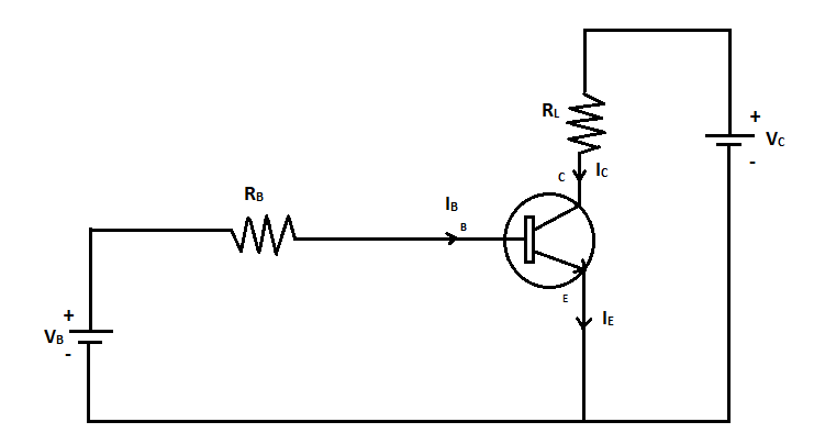
The circuit diagram of NPN transistor in common emitter configuration is given below
Working:
Here the base and the collector are connected to the positive terminals of the cell and the emitter is connected to the negative terminal of the cell. The electrons from the emitter flow towards the base resulting in an emitter current ${I_E}$. As the base is lightly doped and very thin, a few electrons combine with holes at the base. For every hole neutralized, an electron enters the positive terminal of the battery. This constitutes the base current ${I_B}$. The balanced electrons cross the base region and reach the collector region. These electrons move to the positive of the battery ${V_C}$. This constitutes the collector current ${I_C}$. Thus the emitter current is the sum of collector current and base current.
${I_E} = {I_B} + {I_C}$
As the collector current depends on the base current, the transistor action can be controlled by controlling the base current . The base current is of the order of microamperes whereas the collector current is of the order of milliamperes. The emitter current and the collector current are almost equal as the base current is very small.
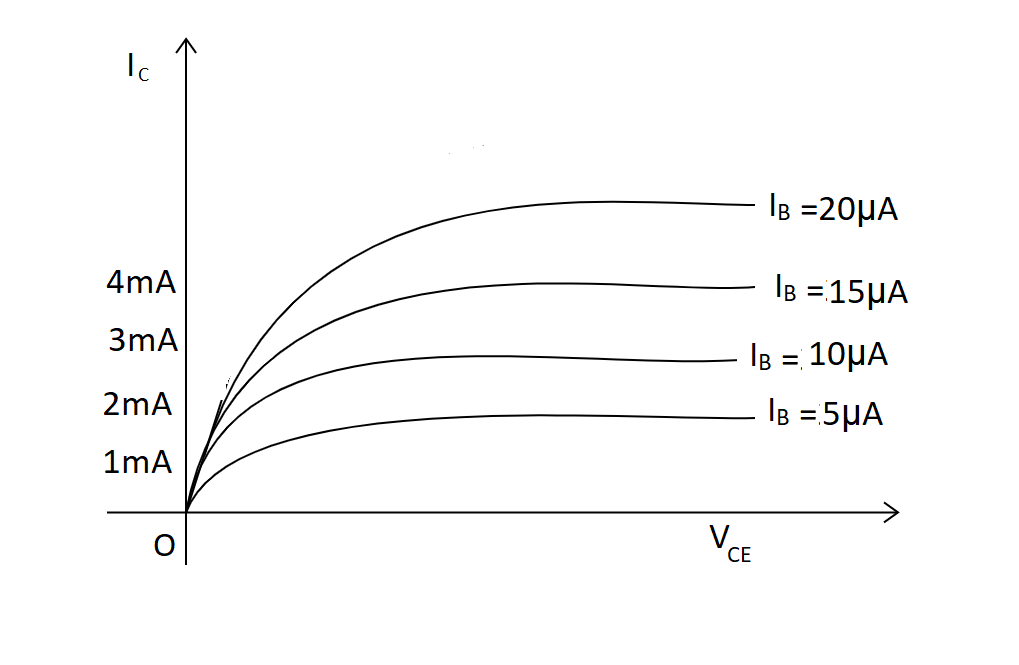
A graph is plotted with collector current ${I_C}$ along Y-axis and collector emitter voltage ${V_{CE}}$ along X-axis keeping ${I_B}$ constant. The procedure is repeated for different values of ${I_B}$. A family of output characteristic curves is obtained as shown.
Note:
As the collector-base region is reverse biased, its resistance is very high compared to the emitter-base region. Hence a greater amount of power is developed at the base collector region than that at the base emitter region. This produces an amplifying action for voltage or power.
Complete step by step solution:
The circuit diagram of NPN transistor in common emitter configuration is given below
Working:
Here the base and the collector are connected to the positive terminals of the cell and the emitter is connected to the negative terminal of the cell. The electrons from the emitter flow towards the base resulting in an emitter current ${I_E}$. As the base is lightly doped and very thin, a few electrons combine with holes at the base. For every hole neutralized, an electron enters the positive terminal of the battery. This constitutes the base current ${I_B}$. The balanced electrons cross the base region and reach the collector region. These electrons move to the positive of the battery ${V_C}$. This constitutes the collector current ${I_C}$. Thus the emitter current is the sum of collector current and base current.
${I_E} = {I_B} + {I_C}$
As the collector current depends on the base current, the transistor action can be controlled by controlling the base current . The base current is of the order of microamperes whereas the collector current is of the order of milliamperes. The emitter current and the collector current are almost equal as the base current is very small.
A graph is plotted with collector current ${I_C}$ along Y-axis and collector emitter voltage ${V_{CE}}$ along X-axis keeping ${I_B}$ constant. The procedure is repeated for different values of ${I_B}$. A family of output characteristic curves is obtained as shown.
Note:
As the collector-base region is reverse biased, its resistance is very high compared to the emitter-base region. Hence a greater amount of power is developed at the base collector region than that at the base emitter region. This produces an amplifying action for voltage or power.
Recently Updated Pages
JEE Main 2023 April 6 Shift 1 Question Paper with Answer Key
JEE Main 2023 April 6 Shift 2 Question Paper with Answer Key
JEE Main 2023 (January 31 Evening Shift) Question Paper with Solutions [PDF]
JEE Main 2023 January 30 Shift 2 Question Paper with Answer Key
JEE Main 2023 January 25 Shift 1 Question Paper with Answer Key
JEE Main 2023 January 24 Shift 2 Question Paper with Answer Key
Trending doubts
JEE Main 2026: Session 2 Registration Open, City Intimation Slip, Exam Dates, Syllabus & Eligibility
JEE Main 2026 Application Login: Direct Link, Registration, Form Fill, and Steps
Understanding the Angle of Deviation in a Prism
Hybridisation in Chemistry – Concept, Types & Applications
How to Convert a Galvanometer into an Ammeter or Voltmeter
Understanding Uniform Acceleration in Physics
Other Pages
JEE Advanced Marks vs Ranks 2025: Understanding Category-wise Qualifying Marks and Previous Year Cut-offs
Dual Nature of Radiation and Matter Class 12 Physics Chapter 11 CBSE Notes - 2025-26
Understanding the Electric Field of a Uniformly Charged Ring
JEE Advanced Weightage 2025 Chapter-Wise for Physics, Maths and Chemistry
Derivation of Equation of Trajectory Explained for Students
Understanding Electromagnetic Waves and Their Importance