


Draw the typical input and output characteristics of a $n - p - n$ transistor in $CE$ configuration. Show how these characteristics can be used to determine
(a) the input resistance ( ${r_i}$ ) and
(b) current amplification factor $\left( \beta \right)$ .
Answer
232.8k+ views
Hint: The $n - p - n$ transistor has the input, output and the transfer characteristics. Draw the input characteristics between base current and base emitter voltage and the output characteristics between the collector current and the common emitter voltage.
Complete step by step solution:
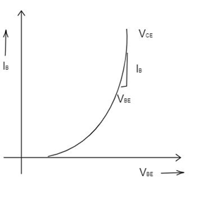
(a) The input resistance is also known as input impedance. It is defined as the ratio of the changes in the base emitter voltage to the corresponding change in the base current at a given particular common emitter voltage in the transistor.
The formula of the input impedance is given by
${r_i} = \dfrac{{\Delta {V_{BE}}}}{{\Delta {I_B}}}$ ( at a given ${V_{CE}}$ )
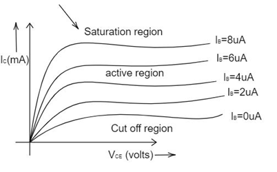
(b) The term current amplification factor is also known as the current gain. It is obtained by dividing the small change in the collector current to that of the corresponding change in the base current of the transistor at constant common emitter voltage.
The formula of the current amplification factor is given by
$\beta = \dfrac{{\Delta {I_C}}}{{\Delta {I_B}}}$ ( at a given ${V_{CE}}$ )
The following graph represents the input characteristics of the $n - p - n$ transistor. It shows that to a certain point, when the base current increases the base emitter voltage remains the same.
The following graph shows the output characteristics of the $n - p - n$ transistor. It includes the cut off, active and the saturated regions of the base current where the common emitter voltage is constant.
Note: In the $n - p - n$ transistor, the $P$ - type of the semiconductor is made connected between the $N$ - type of the semiconductor. It is most commonly used and it looks like the $PN$ junction diode connected back to back. In this transistor, the electron transfers from the base to the collector.
Complete step by step solution:
(a) The input resistance is also known as input impedance. It is defined as the ratio of the changes in the base emitter voltage to the corresponding change in the base current at a given particular common emitter voltage in the transistor.
The formula of the input impedance is given by
${r_i} = \dfrac{{\Delta {V_{BE}}}}{{\Delta {I_B}}}$ ( at a given ${V_{CE}}$ )
(b) The term current amplification factor is also known as the current gain. It is obtained by dividing the small change in the collector current to that of the corresponding change in the base current of the transistor at constant common emitter voltage.
The formula of the current amplification factor is given by
$\beta = \dfrac{{\Delta {I_C}}}{{\Delta {I_B}}}$ ( at a given ${V_{CE}}$ )
The following graph represents the input characteristics of the $n - p - n$ transistor. It shows that to a certain point, when the base current increases the base emitter voltage remains the same.
The following graph shows the output characteristics of the $n - p - n$ transistor. It includes the cut off, active and the saturated regions of the base current where the common emitter voltage is constant.
Note: In the $n - p - n$ transistor, the $P$ - type of the semiconductor is made connected between the $N$ - type of the semiconductor. It is most commonly used and it looks like the $PN$ junction diode connected back to back. In this transistor, the electron transfers from the base to the collector.
Recently Updated Pages
JEE Main 2023 April 6 Shift 1 Question Paper with Answer Key
JEE Main 2023 April 6 Shift 2 Question Paper with Answer Key
JEE Main 2023 (January 31 Evening Shift) Question Paper with Solutions [PDF]
JEE Main 2023 January 30 Shift 2 Question Paper with Answer Key
JEE Main 2023 January 25 Shift 1 Question Paper with Answer Key
JEE Main 2023 January 24 Shift 2 Question Paper with Answer Key
Trending doubts
JEE Main 2026: Session 2 Registration Open, City Intimation Slip, Exam Dates, Syllabus & Eligibility
JEE Main 2026 Application Login: Direct Link, Registration, Form Fill, and Steps
Understanding the Angle of Deviation in a Prism
Hybridisation in Chemistry – Concept, Types & Applications
How to Convert a Galvanometer into an Ammeter or Voltmeter
Understanding Uniform Acceleration in Physics
Other Pages
JEE Advanced Marks vs Ranks 2025: Understanding Category-wise Qualifying Marks and Previous Year Cut-offs
Dual Nature of Radiation and Matter Class 12 Physics Chapter 11 CBSE Notes - 2025-26
Understanding the Electric Field of a Uniformly Charged Ring
JEE Advanced Weightage 2025 Chapter-Wise for Physics, Maths and Chemistry
Derivation of Equation of Trajectory Explained for Students
Understanding Electromagnetic Waves and Their Importance