


When an input signal \[1\] is applied to a NOT gate, its output is:
A) \[1\]
B) \[0\]
C) Either \[0\] or \[1\]
D) Both \[0\] and \[1\]
Answer
232.8k+ views
Hint: NOT gate is one of the basic logical gates. It can be remembered from the name itself that NOT implies getting the opposite output. Remember all the basic gates to avoid confusion.
Complete step by step solution:
The various basic logic gates used digital systems are as follows:
1. OR Gate
2. AND Gate
3. NOT Gate
4. XOR Gate
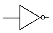
Below is the NOT gate.
OR GATE: In OR gate the output of an OR gate gives the state \[1\] , if one or more inputs attain the state \[1\] i.e. when any one input is \[1\] then the output will be one.
The Boolean expression of the OR gate is given as \[Y=A+B\], which is read as \[Y\] equals \[A\] ‘\[OR\] ’ \[B\].
AND GATE: In AND gate the output of an AND gate is \[1\] if and only if all the inputs are in state \[1\]. The Boolean expression of AND gate is \[Y=A.B\] which is read as Y equals A ‘AND’ B.
NOT GATE: In NOT gate the output of a NOT gate attains the state \[1\] if and only if the input does not attain the state \[1\] . The Boolean expression is \[Y=\overline{A}\] , read as Y equals NOT A.
Hence for input signal \[1\] the output will be \[0\].
Note: All basic gates must be remembered. NAND and XNOR gates are the logical gates which can be obtained using the basic OR, NOT and AND gate. Also the truth table can be easily constructed for each logical gate based on the above definitions. Truth tables make it easier to understand logical gates.
Complete step by step solution:
The various basic logic gates used digital systems are as follows:
1. OR Gate
2. AND Gate
3. NOT Gate
4. XOR Gate
Below is the NOT gate.
OR GATE: In OR gate the output of an OR gate gives the state \[1\] , if one or more inputs attain the state \[1\] i.e. when any one input is \[1\] then the output will be one.
The Boolean expression of the OR gate is given as \[Y=A+B\], which is read as \[Y\] equals \[A\] ‘\[OR\] ’ \[B\].
AND GATE: In AND gate the output of an AND gate is \[1\] if and only if all the inputs are in state \[1\]. The Boolean expression of AND gate is \[Y=A.B\] which is read as Y equals A ‘AND’ B.
NOT GATE: In NOT gate the output of a NOT gate attains the state \[1\] if and only if the input does not attain the state \[1\] . The Boolean expression is \[Y=\overline{A}\] , read as Y equals NOT A.
Hence for input signal \[1\] the output will be \[0\].
Note: All basic gates must be remembered. NAND and XNOR gates are the logical gates which can be obtained using the basic OR, NOT and AND gate. Also the truth table can be easily constructed for each logical gate based on the above definitions. Truth tables make it easier to understand logical gates.
Recently Updated Pages
JEE Main 2023 April 6 Shift 1 Question Paper with Answer Key
JEE Main 2023 April 6 Shift 2 Question Paper with Answer Key
JEE Main 2023 (January 31 Evening Shift) Question Paper with Solutions [PDF]
JEE Main 2023 January 30 Shift 2 Question Paper with Answer Key
JEE Main 2023 January 25 Shift 1 Question Paper with Answer Key
JEE Main 2023 January 24 Shift 2 Question Paper with Answer Key
Trending doubts
JEE Main 2026: Session 2 Registration Open, City Intimation Slip, Exam Dates, Syllabus & Eligibility
JEE Main 2026 Application Login: Direct Link, Registration, Form Fill, and Steps
Understanding the Angle of Deviation in a Prism
Hybridisation in Chemistry – Concept, Types & Applications
How to Convert a Galvanometer into an Ammeter or Voltmeter
Understanding Uniform Acceleration in Physics
Other Pages
JEE Advanced Marks vs Ranks 2025: Understanding Category-wise Qualifying Marks and Previous Year Cut-offs
Dual Nature of Radiation and Matter Class 12 Physics Chapter 11 CBSE Notes - 2025-26
Understanding the Electric Field of a Uniformly Charged Ring
JEE Advanced Weightage 2025 Chapter-Wise for Physics, Maths and Chemistry
Derivation of Equation of Trajectory Explained for Students
Understanding Electromagnetic Waves and Their Importance