Courses
Courses for Kids
Free study material
Offline Centres
More
Store Icon
Store

Electronic Devices Chapter - Physics JEE Main

ffImage
hightlight icon
highlight icon
highlight icon
share icon
copy icon
SearchIcon

Concepts of Electronic Devices for JEE Main Physics

A smart way of preparation will help students in securing good grades in competitive exams like IIT-JEE and JEE-Main. ‘Electronic devices’ is one such important chapter that will definitely help students in securing good scores and boost their grades in the upcoming exams.


The electronic devices chapter introduces us to what is electronics and the types of electronics. The chapter includes the concepts of semiconductor physics. In this chapter, students will have exposure to the concepts of the conduction of electrons in different material types. We study the differences between the conductor, semiconductor and insulators with the help of the energy gap between the covalent and valence band. Further, in this chapter, we study the semiconductor and types of semiconductors classification depending on the doping method (Intrinsic and Extrinsic). 


In electronic devices, we study a few most important semiconductor devices such as diodes, and transistors in detail. At last, we will be moving towards digital electronics which is the fundamental and most interesting part of the chapter.


In this article, students will be provided with the content that will be a helping aid for their preparation. Let's start!!

JEE Main Physics Chapters 2024 


Important Topics of Electronic Devices Chapter

  • Semiconductors

  • Energy Bands In Solids 

  • Classification of Materials

  • PN-Junction diode

  • Biasing Techniques

  • PN-Junction Diode As A Rectifier

  • Zener Diodes

  • Transistors-NPN and PNP

  • Transistor As an Oscillator

  • Logic Gates

  • De Morgan Theorems


Electronic Devices Important Concept of JEE Main

Concept Name

Key Points

Energy Bands in Solids

  • Valence Band: It is the band formed by the outermost electrons (valence electrons) which are strongly bound to the nuclei.

  • Conduction Band: It is the band formed by the free electrons (conduction electrons) which are loosely bound to the nuclei.

Forbidden Energy Gap

  • Energy gap in any solid is the separation between the conduction and valence band

Classification of materials

  • Conductors: These are the semiconductor materials in which there will be a very small energy gap or no energy gap between the CB and VB

  • Insulators: These are the solid materials in which the energy bandgap will be large enough, such that conduction will not be taking place.

  • Semiconductors: These are the materials whose conductivity lies between conductors and insulators. The energy gap between these will be small but more than the conductors. Some of the Semiconductor electrical devices examples are transistors, diodes, etc…

Types of Semiconductors

  • Intrinsic Semiconductors: Intrinsic semiconductors are the pure form of semiconductors. Ge and Si are examples.

  • Extrinsic Semiconductors: These are the type of semiconductors in which impurities will be added. Extrinsic semiconductors are further classified as N-type and P-type semiconductors.

N-type and P-type Semiconductors

  • N-type: These are the semiconductors formed by adding pentavalent impurities to the pure semiconductor. Here, electrons will be the majority charge carriers.

  • P-type: These are the semiconductors formed by adding trivalent impurities to the pure semiconductors. Here, holes will be the majority charge carriers.

PN-Junction Diode

  • It is a two-terminal electronic device that helps in regulating the flow of electric current.

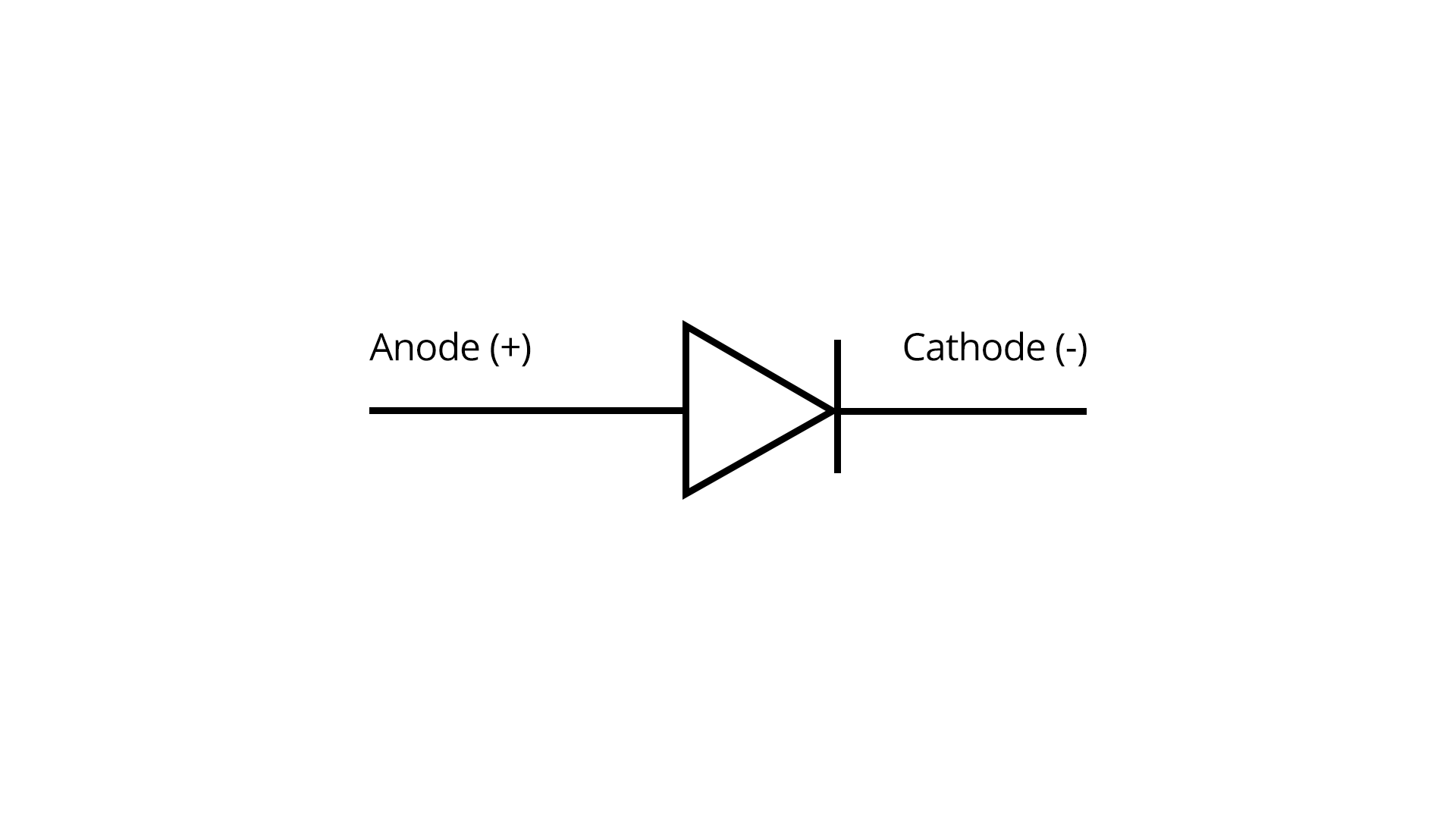
  • The symbol of the PN-Junction diode is:


The symbol of the PN-Junction diode

Biasing Methods

  • Forward biasing: If the positive terminal of an electronic device is connected to the positive and negative terminal, the negative terminal of the battery is known as forward biasing.

So, in forward bias, the diode allows current to flow easily.

The current (I) through the diode is given by the Shockley diode equation:

$I = I_0 e^{\dfrac{qV}{kT}} - 1$

  • Reverse biasing: If the positive terminal of an electronic device is connected to the negative and negative terminal connected to the positive terminal of the battery is known as reverse biasing.

So, in reverse bias, the diode blocks the current efficiently.

A small reverse current, known as reverse leakage current, flows, which is governed by the diode's characteristics and temperature.

Diode As a Rectifier

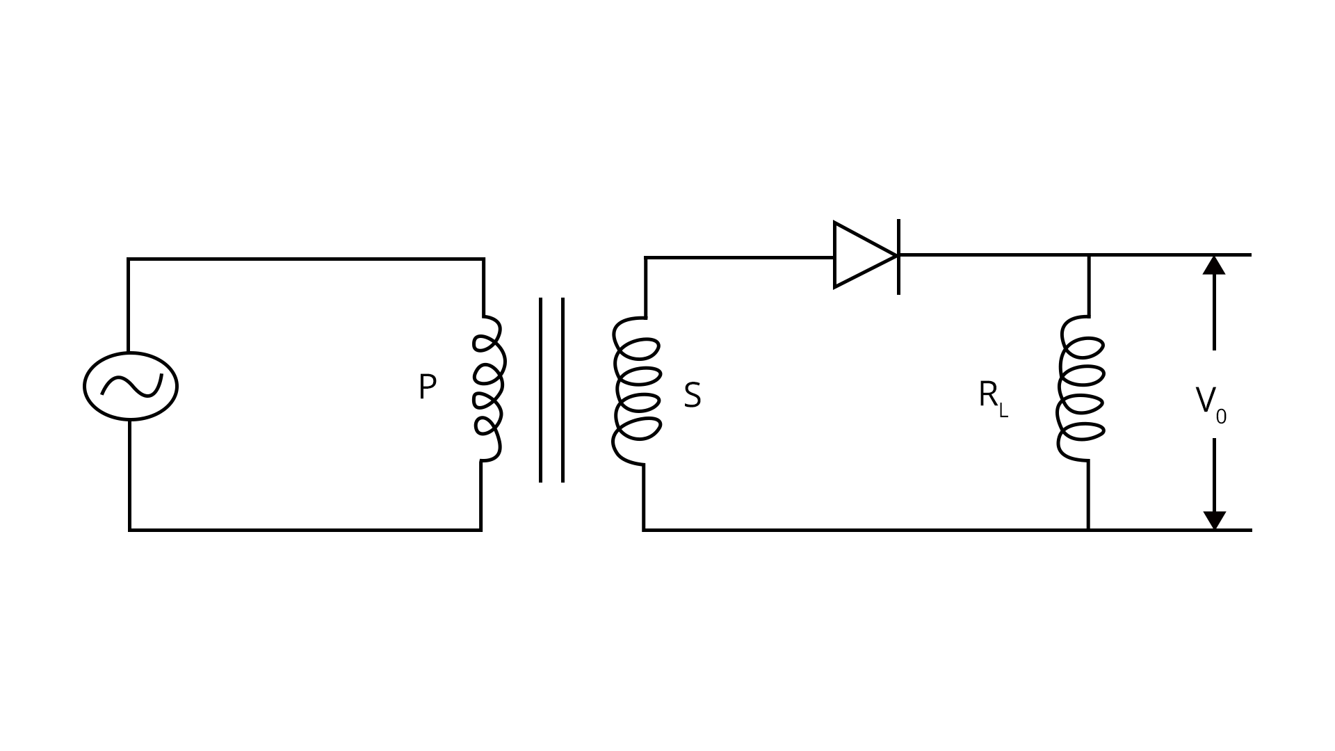
Rectifiers: These are the electronic devices used for converting alternating current into direct current.

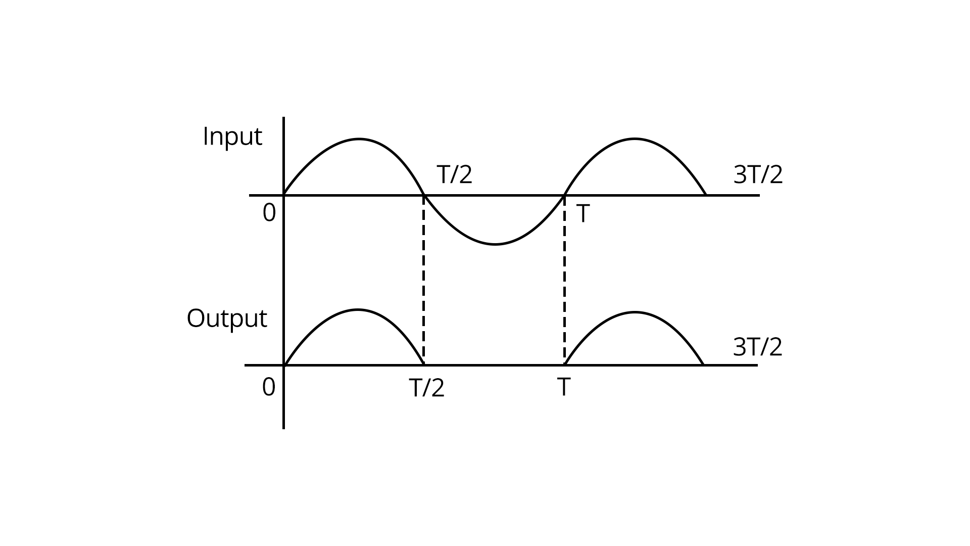
Half Wave Rectifier

Only half part of the ac signal will be rectified.


Rectifiers

Half Wave Rectifier

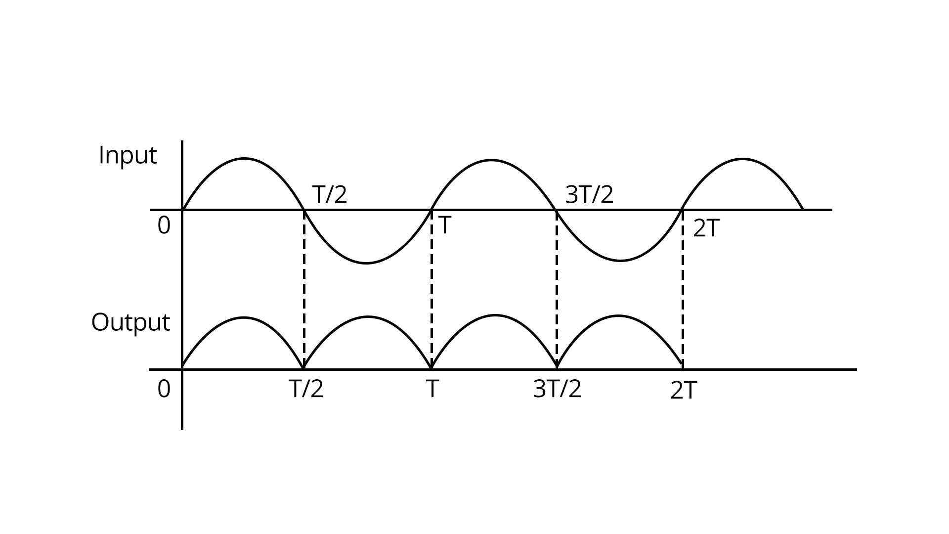
Full Wave Rectifier

The complete cycle of the ac signal will be converted into a dc signal.

dc signal

Full Wave Rectifier


I-V Characteristics of LED

  • Light Emitting Diodes (LEDs) are diodes that emit light when current flows through them. Their I-V characteristics differ from regular diodes. The voltage-current relationship for an LED is given by:

$I = I_s e^{\dfrac{qV}{nkT}} - 1$

  • Here, I_s is the saturation current, V is the voltage, n is the emission coefficient, and k and T have their previous meanings.

Photodiode, Solar Cell, and Zener Diode

  • Photodiode: A photodiode is a semiconductor device that converts light into electrical current. The photocurrent generated is directly proportional to the incident light intensity. It operates in reverse bias, and its reverse current increases with increasing light intensity.

  • Solar Cell: A solar cell is a photovoltaic device that converts sunlight into electricity. It works on the same principle as a photodiode but is designed to produce a significant amount of power.

  • Zener Diode: A Zener diode operates in reverse bias, just like a regular diode. However, it is designed to work in the breakdown region, known as the Zener breakdown. It maintains a constant voltage across its terminals and is often used as a voltage regulator.

Zener Diode as a Voltage Regulator

  • The voltage across a Zener diode is given by:

$V_{z}=V_{Z0}+(IR_{z}) V_{z}$

  • Where $V_{z0}$ is the Zener voltage, I is the current, and $R_z$ is the dynamic resistance.

Transistors

  • These are the three-terminal electronic devices used for the amplification process.

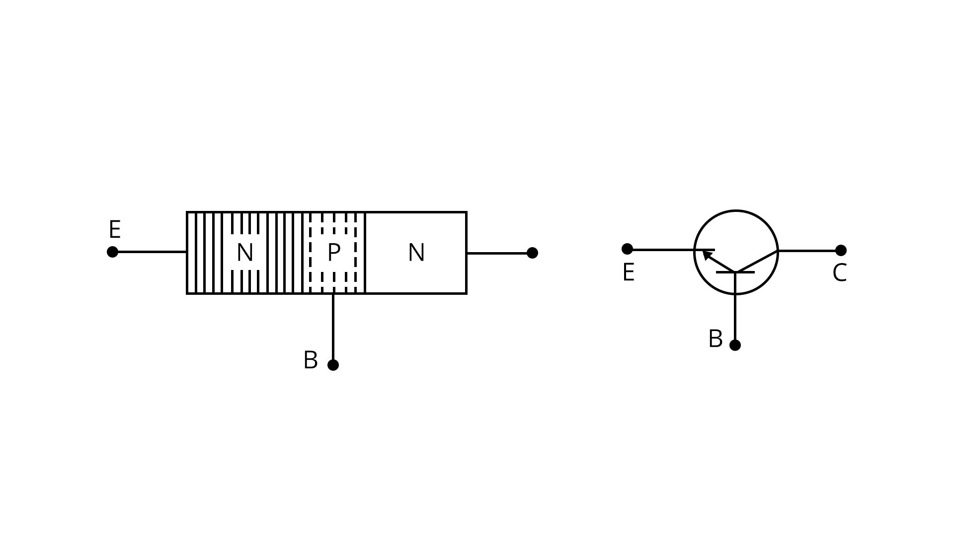
  • Transistors consist of an emitter, base and collector.


Transistors


  • A transistor is made by sandwiching two pn-junction diodes back to back.

  • There are two types of transistors PNP and NPN, depending on the majority charge carriers.


Transistor as an Amplifier, Oscillator, and as Switch


  • Transistor as an Amplifier: In the common emitter configuration, the transistor amplifies the input signal. The voltage gain (Av) is given by:

$Av = -\beta \times \dfrac{Rc}{(Re + (1 + \beta) Re)}$

  • Transistor as an Oscillator: A transistor can also function as an oscillator, generating periodic signals. It does so by utilizing positive feedback.

  • Transistor as a Switch: Transistors can be used as electronic switches, where a small signal at the base controls a much larger current flow between the collector and emitter. This switching capability is essential in digital logic and power control applications.

Logic gates

  • Logic gates are the building blocks of digital electronics. 

  • The logic gates are basically the devices used to perform mathematical operations using bits 0 and 1. 

  • Logic gates are two or more inputs and single output devices.

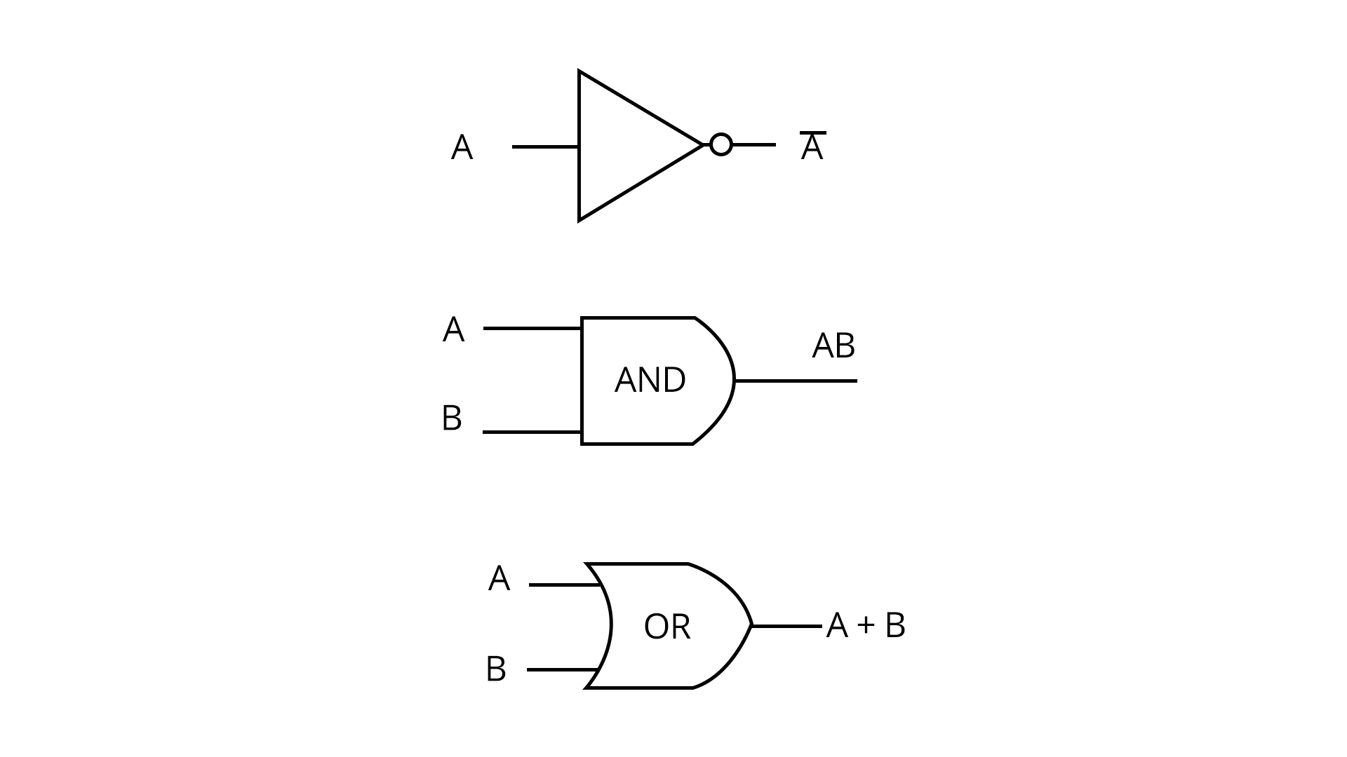
  • There are three basic gates: OR, AND and NOT.

  • Two universal gates: NAND Aand NOT


Basic Logic Gates

  • OR Gate: These are the logic gates used to perform addition.

    • Boolean expression: 

Y= A+B

  • AND Gate: These are the logic gates used to perform multiplication.

    • Boolean expression: 

Y= AB

  • NOT Gate: These are the logic gates used to perform complementary functions.

    • Boolean expression: 

$Y=\bar A$


Basic Logic Gates

Universal Logic Gates

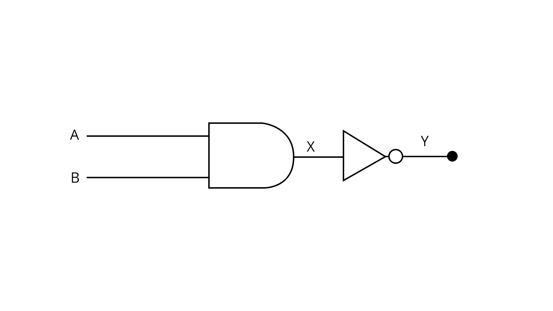
  • NAND Gate: It is the combination of NOT and AND gates.

$Y= \bar {AB}$


Combination of NOT and AND gates


  • NOR Gate: It is the combination of NOT and OR gates.

$Y=Y=\overline{A+B}$


Combination of NOT and OR gates


Types of Transistors:

Transistors come in two main types: NPN transistors and PNP transistors.


NPN Transistor:

An NPN transistor has a thin P layer sandwiched between two thick N layers.


PNP Transistor:

For a PNP transistor, a thin N layer is sandwiched between two thick P layers.


Logic Gates:

Logic gates show the logical relationship between input and output voltage. A truth table lists all possible combinations of inputs and outputs.


Basic Logic Gates:

The three basic logic gates are AND, OR, and NOT.


AND Gate:

In an AND gate, if all inputs are high, the gate goes to the high state. For example, if both A and B are true, the output (Y) is true (Y = A.B).


The Truth Table of AND:


A

B

Y

0

0

0

0

1

0

1

0

0

1

1

1


Doping Semiconductor Material

Doping process highly increases the number of charge carriers within the crystal. If a doped semiconductor material contains more free holes it is called "p-type", and when it contains more free electrons it is known as "n-type".


N-type (e.g. Doped with Antimony)

In N-type semiconductors the characteristics are as follows:

1. The Donors are positively charged.

2. A large number of free electrons.

3. A small number of holes in relation to the number of free electrons.

4. Doping gives positively charged donors and negatively charged free electrons.

5. Supply of energy gives negatively charged free electrons and positively charged holes.


P-type (e.g. Doped with Boron) 

In these, types of materials have characteristics as follows:

1. The Acceptors are negatively charged.

2. There are a large number of holes.

3. A small number of free electrons in relation to the number of holes.

4. Doping gives negatively charged acceptors and-positively charged holes.

5. Supply of energy gives positively charged holes and negatively charged free electrons.


Properties of Semiconductors

Under ideal conditions or circumstances, semiconductor devices are able to conduct electricity. However, there are a number of other attributes to consider.


  • An increase in temperature (applying heat) results in an increase in the conductivity of the semiconductor.

  • Electrons and holes flow along the semiconductor.

  • This results in reduced power loss.

  • Performing doping increases the efficiency of semiconductor devices.

  • As the temperature rises, resistance decreases.


Examples of Semiconductor Devices

Examples of Two-terminal Semiconductor

Examples of Three-terminal Semiconductor

DIAC

TRIAC

PIN Diode

Field Effect Transistor

Tunnel Diode

Darlington Transistor

Laser Diode

Thyristor

Schottky Diode

Silicon Controlled Rectifier (SCR)

Zener Diode

Unijunction Transistor


List of Important Formulas for Electronic Devices Chapter

Sl. No

Concept Name

Formula

1. 

Mass Action Law

The product of the concentrations of free electrons 'ne' and holes 'nh' is a constant in thermal equilibrium, and it is independent of the amount of doping by acceptor and donor impurities.

${n_e}\times {n_h}={n_i}^2$

2. 

Form Factor

For Full Wave Rectifier:

$F=\dfrac {\pi}{2\sqrt {2}}$


For Half Wave Rectifier:

$F=\dfrac {\pi}{2}$

3.

RMS Value of Current

$I_{rms}=\sqrt {{I_{dc}}^2 +{I_{ac}}^2}$

4. 

Ripple Factor

$r=\dfrac {I_{ac}}{I_{dc}}=\sqrt {{F^2}-1}$

5.

Electrical conductivity of semiconductors

Intrinsic semiconductor:-

  • σ = e(neμe + nhμh)

  • $\sigma={\sigma_o}e^{\dfrac {E_g}{kT}}$


Extrinsic semiconductor:-

  • N-type: σ = eneμe

  • P-type: σ = ennμn

6.

Transistors

Relation between the currents in the transistors:

IE=IC+IB (IB << IE, IB<<IC)

Current gain

$\alpha=\dfrac {I_C}{I_E}$

$\beta=\dfrac {I_C}{I_B}$

7. 

Relation Between the and

$\alpha=\dfrac {\beta}{1+\beta}$ and

$\beta=\dfrac {\alpha}{1-\alpha}$

8.

Voltage gain

$A_v=\dfrac {V_{out}}{V_{in}}$

9.

De Morgan’s Theorems

$\overline{A+B}=\bar {A} . \bar {B}$

$\overline{A.B}=\bar {A} + \bar {B}$

10.

Miscellaneous Formulae

Triodes: A vacuum tube containing three elements namely plate, filament and grid.

Plate resistance (rp):

$r_p=\left (\dfrac {\Delta {V_P}}{\Delta {I_P}}\right)_{{V_g}=Constant}$

Mutual Inductance (gm): 

$g_m=\left (\dfrac {\Delta {I_P}}{\Delta {V_g}}\right)_{{V_P}=Constant}$


JEE Main Electronic Devices Solved Examples

  1. Draw and explain the output waveform across the load resistor R, if the input waveform is as shown in the given figure.


Waveform


Sol:

Given,

A square wave is used as a signal, now we are asked to determine the output waveform when the signal is passed through the load resistor R.

Here, we will consider two different conditions:

  1. When the input signal +5V: 

With +5 V input, the pn-junction diode will be forward biased and +5 V voltage will pass through the load resistance.

  1. When the input signal -5V: 

With -5 V input, the pn-junction diode will be reverse biased and no voltage will pass through the load resistance.

Therefore, the output waveform will be as shown below:


Waveform


Key Point: When the pn-junction diode is reverse biased the voltage across the resistor will be zero.


  1. In an unbiased p-n junction diode, holes tend to diffuse from the p-region to n-region, due to

    1. hole concentration in p-region is more as compared to n-region.

    2. they move across the junction by the potential difference.

    3. free electrons in the n-region attract them.

    4. All the above

Sol: 

The right answer is option a.

Reason: In an unbiased pn junction diode, holes tend to diffuse from the p-region to n-region, because, in p-region is having abundant holes which will attract the electrons in the n-region.

Key point: The charge carriers always move from higher concentration to lower concentration. In this question, we can see that p-region having more number of holes than in n-region.


Previous Year Questions From Electronic Devices

  1. Identify the logic operation carried out by the given circuit


Logic Operation


  1. OR

  2. AND

  3. NOR

  4. NAND

Sol:

Given, 


Logic Circuit


On analysing the logic circuit we found that,

$Z=\bar {A}. \bar {B}=\overline{A+B}$= NOR gate

Therefore, Option C is the right answer.

Trick: Whenever we come across a complimentary function we should remember that De morgan’s theorem will solve the equation easily.


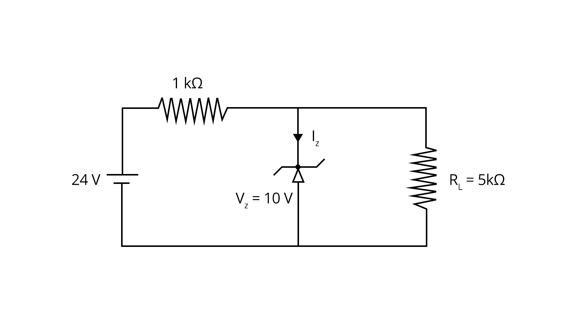
  1. For the given circuit, the power across zener diode is ………..mW.


Zener Diode


Sol:

Given, an electric circuit with zener diode. Now we are asked to determine the power across the zener diode.


seo images


Let us solve the circuit first:

$I_L=\dfrac {10}{5}=2 mA$

I=141=14 mA$I=\dfrac {14}{1}=14 mA$

$I_Z=I-{I_L}=14-2=12 mA$

Therefore, power across zener diode is:

$P_Z = {I_Z}{V_Z}=12 mA \times 10=12o mW$


Trick: Voltage across the parallel components will always be equal.


Practice Questions From Electronic Devices

  1. In a pure, or intrinsic, semiconductor, valence band holes and conduction-band electrons are always present 

  1. None of these

  2. such that number of holes is greater than the number of electrons

  3. in equal numbers

  4. such that number of electrons is greater than the number of holes

(Ans: Option C)


  1. When Ge crystal is doped with phosphorus atoms, it becomes

  1. superconductor

  2. Insulator

  3. n-type

  4. p-type

(Ans: Option C)


JEE Main Physics Electronic Devices Study Materials

Here, you'll find a comprehensive collection of study resources for Electronic Devices designed to help you excel in your JEE Main preparation. These materials cover various topics, providing you with a range of valuable content to support your studies. Simply click on the links below to access the study materials of Electronic Devices and enhance your preparation for this challenging exam.


JEE Main Physics Study and Practice Materials

Explore an array of resources in the JEE Main Physics Study and Practice Materials section. Our practice materials offer a wide variety of questions, comprehensive solutions, and a realistic test experience to elevate your preparation for the JEE Main exam. These tools are indispensable for self-assessment, boosting confidence, and refining problem-solving abilities, guaranteeing your readiness for the test. Explore the links below to enrich your Physics preparation.


Benefits of Using Vedantu for JEEMain 2024 Exam - Physics Electronic Devices

Electronic Devices chapter for JEE Main 2024 with Vedantu: where clear conceptual understanding, focused exam preparation, and expert guidance converge to optimize your learning experience. Accessible study materials, interactive learning, efficient time management, realistic exam simulations, and a personalised approach await, ensuring a holistic preparation for success in the Physics section. Let's explore more on how Vedantu can help in JEE Main preparation:


  1. Clear Conceptual Understanding: Vedantu ensures a lucid comprehension of the "Electronic Devices" chapter for JEE Main 2024, simplifying intricate concepts, making them easily understandable.

  2. Focused Exam Preparation: Our platform provides specific resources targeting the "Electronic Devices" chapter, including important questions and exam tips, enabling students to concentrate on vital topics for efficient exam preparation.

  3. Expert Guidance: Vedantu offers expert guidance from experienced teachers, aiding students in navigating the complexities of the "Electronic Devices" chapter efficiently and addressing any doubts they may encounter.

  4. Accessible Study Material: Comprehensive study materials, notes, and solutions related to the "Electronic Devices" chapter are readily available, supporting self-paced learning and effective revision.

  5. Interactive Learning: The interactive learning environment on Vedantu facilitates engagement with the concepts of "Electronic Devices" in Physics, enhancing understanding and retention through active participation.

  6. Efficient Time Management: Vedantu's resources assist in optimizing study time, ensuring that students cover essential topics within the "Electronic Devices" chapter, preparing them thoroughly for the JEE Main 2024 Physics section.

  7. Realistic Exam Simulation: Practice tests and mock exams provided by Vedantu simulate real exam conditions for the "Electronic Devices" chapter, allowing students to familiarize themselves with the exam format and build confidence.

  8. Personalised Learning Experience: Vedantu tailors its approach to cater to individual learning styles, offering a personalised learning experience specifically designed for better assimilation of concepts within the "Electronic Devices" chapter for JEE Main 2024.


Conclusion

In this article, we dove into the exciting world of Electronic Devices in your JEE Main physics chapter. We covered all the essential concepts and solutions to common questions you might encounter. You'll discover the ins and outs of electronic components and how they work together to create various electronic devices. We've also got easy-to-understand PDFs for you to download, which will help you grasp these concepts and be well-prepared for your exams. So, get ready to explore the fascinating realm of Electronic Devices, and ace your physics exam with confidence!

Watch videos on
Electronic Devices Chapter - Physics JEE Main
icon
Semiconductors and Devices for JEE Mains💥 [Complete Theory in One Session👻] IIT JEE Physics |Vedantu
Subscribe
iconShare
5.1K likes
225.7K Views
4 years ago

FAQs on Electronic Devices Chapter - Physics JEE Main

1. Is Semiconductor devices a simple chapter for JEE?

Semiconductors and communication are relatively challenging to deal with. Certain factors must be kept in mind, and your concepts must be clear. You must also memorise a few things in addition to understanding the material. It is a crucial chapter for jee main, and students should study it thoroughly.

2. What is the importance of the electronic devices chapter for JEE?

Minimum of 2-3 questions will appear from this chapter, which covers 3% of the JEE total score. One of the easiest chapters of physics to score in JEE.

3. How to prepare the electronic devices chapter?

Students must prepare for the electronic devices by solving previous year's questions and NCERT solutions.

4. What does the Electronic Devices chapter in Physics cover for JEE Main?

The Electronic Devices chapter in Physics for JEE Main encompasses the study of semiconductor devices, their characteristics, and their applications in electronic circuits. It includes topics like diodes, transistors, amplifiers, and logical gates.

5. How can understanding the Electronic Devices chapter contribute to success in JEE Main Physics?

A solid grasp of the Electronic Devices chapter is crucial for JEE Main success as it forms the foundation for various topics in modern electronics. It helps students comprehend semiconductor physics and electronic circuit applications, ensuring they can tackle related problems in the exam effectively.