


When a forward bias is applied to a p-n junction, it.
Answer
478.5k+ views
Hint: A p-n junction diode device is made when a p-type semiconductor is fused to an n-type semiconductor forming a potential barrier voltage across the diode junction. Generally, it’s a semiconductor device that controls the flow of current in a circuit. In the forward bias condition, a negative voltage is applied on the N-side and is connected with a negative voltage, and P-side is connected with a positive voltage.
Complete answer:
In the p-n junction diode, a depletion region is made due to the recombination of holes and electrons. Electrons from the n side move towards the p side, and holes from the p side move towards the n side to make the depletion region. As a result, an electric field in the opposite direction is formed whenever the external voltage is applied; this is often nothing but barrier potential.
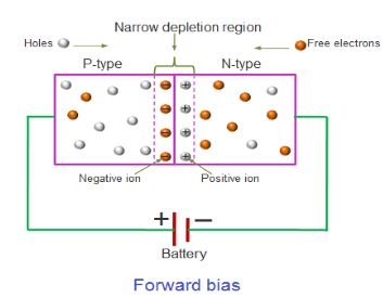
In forward biasing, the p-type is connected with the positive terminal and thus the n-type is connected with the negative terminal of the battery then, the holes in the p-type region and therefore the electrons within the n-type region are pushed towards the junction which reduces the width of the depletion layer. Also the distance between the diffused holes and electrons decreases which ends up in a decrease in field within the depletion region. Hence, the potential barrier decreases.
Note: The width of the depletion layer in a p-n junction diode decreases in forward bias because of the repulsion of carriers from battery terminals, holes from p-type, and electrons from n-type. Now, due to the small number of ions within the depletion region, its potential decreases.
Complete answer:
In the p-n junction diode, a depletion region is made due to the recombination of holes and electrons. Electrons from the n side move towards the p side, and holes from the p side move towards the n side to make the depletion region. As a result, an electric field in the opposite direction is formed whenever the external voltage is applied; this is often nothing but barrier potential.
In forward biasing, the p-type is connected with the positive terminal and thus the n-type is connected with the negative terminal of the battery then, the holes in the p-type region and therefore the electrons within the n-type region are pushed towards the junction which reduces the width of the depletion layer. Also the distance between the diffused holes and electrons decreases which ends up in a decrease in field within the depletion region. Hence, the potential barrier decreases.
Note: The width of the depletion layer in a p-n junction diode decreases in forward bias because of the repulsion of carriers from battery terminals, holes from p-type, and electrons from n-type. Now, due to the small number of ions within the depletion region, its potential decreases.
Recently Updated Pages
Master Class 12 Economics: Engaging Questions & Answers for Success
Master Class 12 Physics: Engaging Questions & Answers for Success
Master Class 12 English: Engaging Questions & Answers for Success
Master Class 12 Social Science: Engaging Questions & Answers for Success
Master Class 12 Maths: Engaging Questions & Answers for Success
Master Class 12 Business Studies: Engaging Questions & Answers for Success
Trending doubts
Which are the Top 10 Largest Countries of the World?
What are the major means of transport Explain each class 12 social science CBSE
Draw a labelled sketch of the human eye class 12 physics CBSE
Why cannot DNA pass through cell membranes class 12 biology CBSE
Differentiate between insitu conservation and exsitu class 12 biology CBSE
Draw a neat and well labeled diagram of TS of ovary class 12 biology CBSE