


A p-n junction diode is in reverse bias, then
A. More current flows.
B. The barrier potential decreases.
C. The barrier potential increases.
D. Resistance offered is low.
Answer
588.6k+ views
Hint: The width of the depletion layer in the p-n junction diode will get increased in the reverse bias as charge carriers are attracted into battery terminals, holes from p-type into the negative terminal and the electrons from n-type into the positive terminal.
Complete answer:
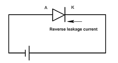
A p-n junction diode is a device in which there are two-terminal or two-electrode semiconductors in it, and also which permits the electric current in only one direction while preventing the electric current in the opposite or reverse direction. The p-n junction, which is made when the p-type and n-type semiconductors are connected together. The symbol of a diode is given as
The width of the depletion layer in the p-n junction diode will get enhanced in the reverse bias because the charge carriers get attracted into battery terminals, holes from p-type into the negative terminal and the electrons from n-type into the positive terminal.
So, the correct answer is “Option B”.
Note:
When we apply a negative voltage which is actually the reverse bias causes the free charges to be pulled away from the junction which is resulted as the increased width of the depletion layer. This has the effect in increasing or decreasing the total resistance of the junction itself allowing or preventing the flow of current through the diodes in PN-junction. Then the depletion layer gets widened with an enhancement of the application of a reverse voltage and narrows with an increase in the giving of a forward voltage. This is because of the differences in their electrical properties on the two sides of the PN junction which results in physical changes.
Complete answer:
A p-n junction diode is a device in which there are two-terminal or two-electrode semiconductors in it, and also which permits the electric current in only one direction while preventing the electric current in the opposite or reverse direction. The p-n junction, which is made when the p-type and n-type semiconductors are connected together. The symbol of a diode is given as
The width of the depletion layer in the p-n junction diode will get enhanced in the reverse bias because the charge carriers get attracted into battery terminals, holes from p-type into the negative terminal and the electrons from n-type into the positive terminal.
So, the correct answer is “Option B”.
Note:
When we apply a negative voltage which is actually the reverse bias causes the free charges to be pulled away from the junction which is resulted as the increased width of the depletion layer. This has the effect in increasing or decreasing the total resistance of the junction itself allowing or preventing the flow of current through the diodes in PN-junction. Then the depletion layer gets widened with an enhancement of the application of a reverse voltage and narrows with an increase in the giving of a forward voltage. This is because of the differences in their electrical properties on the two sides of the PN junction which results in physical changes.
Recently Updated Pages
Master Class 12 Economics: Engaging Questions & Answers for Success
Master Class 12 Physics: Engaging Questions & Answers for Success
Master Class 12 English: Engaging Questions & Answers for Success
Master Class 12 Social Science: Engaging Questions & Answers for Success
Master Class 12 Maths: Engaging Questions & Answers for Success
Master Class 12 Business Studies: Engaging Questions & Answers for Success
Trending doubts
Which are the Top 10 Largest Countries of the World?
What are the major means of transport Explain each class 12 social science CBSE
Draw a labelled sketch of the human eye class 12 physics CBSE
Why cannot DNA pass through cell membranes class 12 biology CBSE
Differentiate between insitu conservation and exsitu class 12 biology CBSE
Draw a neat and well labeled diagram of TS of ovary class 12 biology CBSE