What is the depletion region in a semiconductor diode?
Answer
571.5k+ views
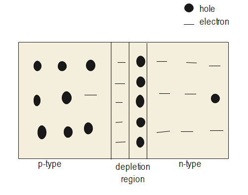
Hint: In this question, we will first discuss the depletion region with diagram, further we will also discuss types of semiconductor. Also, we will see p-type and n-type semiconductor, which will help us for our better understanding.
Complete answer:
As we know that, depletion region is a region in a semiconductor device, or we can say that generally it is at the junction of P-type and N-type materials, in which there is neither an excess of electrons nor of holes.

The free electrons that are crossing the junction from n-side provide extra electrons to the atoms on the p-side by filling holes in the p-side atoms. The atom that gains an extra electron at p-side has more number of electrons than protons. We know that, when the atom gains an extra electron from the outside atom it will become a negative ion.
So, immobile positive charge at negative side or n-side and immobile negative charge at positive side or p-side near the junction acts like a barrier and prevents the flow of free electrons and holes. The region near the junction, here, flow of charge carriers are decreased over a given time and finally results in empty charge carriers or full of immobile charge carriers is called depletion region.
Now, we know that the depletion region is also called the depletion zone or depletion layer or space charge region or space charge layer. Also, the depletion region acts like a wall or barrier between p-type and n-type semiconductor and prevents further flow of free electrons and holes.
Additional information:
As we know that the semiconductors are materials which have conductivity between conductors and nonconductors or insulators. Semiconductors can be pure elements, like silicon or germanium, or compounds such as gallium arsenide or cadmium selenide.
There are two types of semiconductor:
Intrinsic semiconductor: these are pure semiconductors.
Extensive semiconductor: these are semiconductors which are doped or added with impurities. Further, there are n-type and p-type semiconductors.
N-type semiconductor has majority carriers of electrons present and minority of holes, whereas, in p-type semiconductor the majority carriers are holes and minority carriers are electrons.
When both the types of semiconductors are connected, we form a P-N junction. When the majority charge carriers flow towards opposite terminals, we get a region in the middle of the junction.
Thus, we can say that a net negative charge is built at the p-side of p-n junction, it is positively charged. Also, a net positive charge is built at the n-side of the p-n junction.
Here, the net negative charge at p-side of the p-n junction prevents the flow of free electrons crossing from n-side to p-side, as the negative charge present at the p-side of the p-n junction repels the free electrons. Also we can say that the net positive charge at n-side of the p-n junction prevents further flow of holes from p-side to n-side.
Note:
We should remember that large depletion regions inhibit current flow. Also, the distance between the conduction band and valence band is large in the insulator. The distance between the conduction band and valence band in a semiconductor are very small, and can be overcome. Further, there is no distance between the conduction band and valence band.
Complete answer:
As we know that, depletion region is a region in a semiconductor device, or we can say that generally it is at the junction of P-type and N-type materials, in which there is neither an excess of electrons nor of holes.

The free electrons that are crossing the junction from n-side provide extra electrons to the atoms on the p-side by filling holes in the p-side atoms. The atom that gains an extra electron at p-side has more number of electrons than protons. We know that, when the atom gains an extra electron from the outside atom it will become a negative ion.
So, immobile positive charge at negative side or n-side and immobile negative charge at positive side or p-side near the junction acts like a barrier and prevents the flow of free electrons and holes. The region near the junction, here, flow of charge carriers are decreased over a given time and finally results in empty charge carriers or full of immobile charge carriers is called depletion region.
Now, we know that the depletion region is also called the depletion zone or depletion layer or space charge region or space charge layer. Also, the depletion region acts like a wall or barrier between p-type and n-type semiconductor and prevents further flow of free electrons and holes.
Additional information:
As we know that the semiconductors are materials which have conductivity between conductors and nonconductors or insulators. Semiconductors can be pure elements, like silicon or germanium, or compounds such as gallium arsenide or cadmium selenide.
There are two types of semiconductor:
Intrinsic semiconductor: these are pure semiconductors.
Extensive semiconductor: these are semiconductors which are doped or added with impurities. Further, there are n-type and p-type semiconductors.
N-type semiconductor has majority carriers of electrons present and minority of holes, whereas, in p-type semiconductor the majority carriers are holes and minority carriers are electrons.
When both the types of semiconductors are connected, we form a P-N junction. When the majority charge carriers flow towards opposite terminals, we get a region in the middle of the junction.
Thus, we can say that a net negative charge is built at the p-side of p-n junction, it is positively charged. Also, a net positive charge is built at the n-side of the p-n junction.
Here, the net negative charge at p-side of the p-n junction prevents the flow of free electrons crossing from n-side to p-side, as the negative charge present at the p-side of the p-n junction repels the free electrons. Also we can say that the net positive charge at n-side of the p-n junction prevents further flow of holes from p-side to n-side.
Note:
We should remember that large depletion regions inhibit current flow. Also, the distance between the conduction band and valence band is large in the insulator. The distance between the conduction band and valence band in a semiconductor are very small, and can be overcome. Further, there is no distance between the conduction band and valence band.
Recently Updated Pages
Master Class 12 Economics: Engaging Questions & Answers for Success

Master Class 12 Physics: Engaging Questions & Answers for Success

Master Class 12 English: Engaging Questions & Answers for Success

Master Class 12 Social Science: Engaging Questions & Answers for Success

Master Class 12 Maths: Engaging Questions & Answers for Success

Master Class 12 Business Studies: Engaging Questions & Answers for Success

Trending doubts
Which are the Top 10 Largest Countries of the World?

What are the major means of transport Explain each class 12 social science CBSE

Draw a labelled sketch of the human eye class 12 physics CBSE

Why cannot DNA pass through cell membranes class 12 biology CBSE

Differentiate between insitu conservation and exsitu class 12 biology CBSE

Draw a neat and well labeled diagram of TS of ovary class 12 biology CBSE


