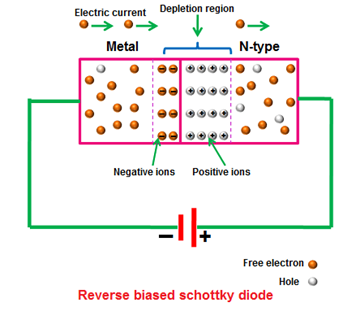
Why does the width of the depletion region increase in reverse bias?
Answer
487.2k+ views
Hint: Let us consider a simple p-n junction diode, a depletion region is a charge-free region that is formed due to diffusion of electrons and holes from n and p regions over to the p and n regions respectively due to a quick junction. The diffusion is continued until a potential barrier sets up in the depletion region that avoids further diffusion. Depletion region is constantly present in the diode but its width is determined by the nature of bias.
Complete answer:
If the battery’s negative terminal is connected to the p-type and the positive terminal of the battery is connected to the n-type, we can say that the diode is reverse biased. Under reverse bias conditions, the holes in the p-type are appealed by the negative terminal of the battery and are pulled away from the junction, similarly by the electrons in the n-type are appealed by the positive terminal of the battery and are pulled away from the depletion region.

Because of this reason, the depletion region increases in a reverse bias. In other words, we can say that when the p-n junction is reversed biased, the positive terminal of the external battery is connected to the n-side of the p-n junction and its negative terminal to the p-side of the p-n junction. The positive terminal of the external battery appeals to the majority of carrier electrons from the n-region and its negative terminal appeals to the majority of carrier holes from the p-region. Because of it, the majority of charge carriers move away from the junction. This increases the width of the depletion layer.
Note:
If we apply forward bias to a P-N junction it boosts the valence electrons of the depletion layer and these electrons start losing their bond. Hence the depletion layer starts collapsing and breaks immediately as it gets a voltage beyond its threshold. When we apply reverse bias the same valence electrons increase due to the merging of both electrons and holes available on either side of the depletion layer in the P and N region. This results in a wide depletion layer up to a limited applied voltage beyond that applied voltage; this layer breaks and produces a sharp or high current flow through the layer.
Complete answer:
If the battery’s negative terminal is connected to the p-type and the positive terminal of the battery is connected to the n-type, we can say that the diode is reverse biased. Under reverse bias conditions, the holes in the p-type are appealed by the negative terminal of the battery and are pulled away from the junction, similarly by the electrons in the n-type are appealed by the positive terminal of the battery and are pulled away from the depletion region.

Because of this reason, the depletion region increases in a reverse bias. In other words, we can say that when the p-n junction is reversed biased, the positive terminal of the external battery is connected to the n-side of the p-n junction and its negative terminal to the p-side of the p-n junction. The positive terminal of the external battery appeals to the majority of carrier electrons from the n-region and its negative terminal appeals to the majority of carrier holes from the p-region. Because of it, the majority of charge carriers move away from the junction. This increases the width of the depletion layer.
Note:
If we apply forward bias to a P-N junction it boosts the valence electrons of the depletion layer and these electrons start losing their bond. Hence the depletion layer starts collapsing and breaks immediately as it gets a voltage beyond its threshold. When we apply reverse bias the same valence electrons increase due to the merging of both electrons and holes available on either side of the depletion layer in the P and N region. This results in a wide depletion layer up to a limited applied voltage beyond that applied voltage; this layer breaks and produces a sharp or high current flow through the layer.
Recently Updated Pages
Master Class 12 Economics: Engaging Questions & Answers for Success

Master Class 12 Physics: Engaging Questions & Answers for Success

Master Class 12 English: Engaging Questions & Answers for Success

Master Class 12 Social Science: Engaging Questions & Answers for Success

Master Class 12 Maths: Engaging Questions & Answers for Success

Master Class 12 Business Studies: Engaging Questions & Answers for Success

Trending doubts
Which are the Top 10 Largest Countries of the World?

What are the major means of transport Explain each class 12 social science CBSE

Draw a labelled sketch of the human eye class 12 physics CBSE

Why cannot DNA pass through cell membranes class 12 biology CBSE

Differentiate between insitu conservation and exsitu class 12 biology CBSE

Draw a neat and well labeled diagram of TS of ovary class 12 biology CBSE


