
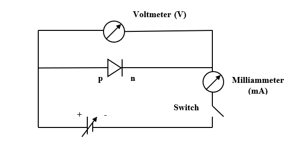
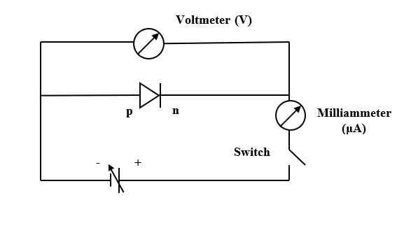
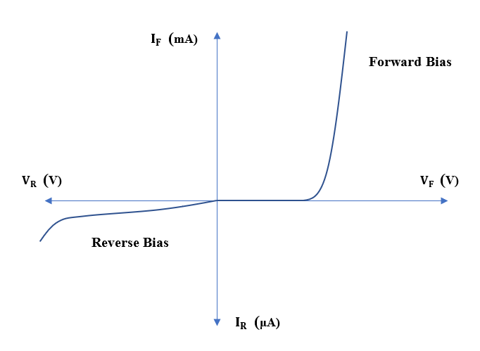
Draw a circuit arrangement for studying V-I characteristics of a p-n junction diode in (a) forward bias and (b) reverse bias. Show typical V-I characteristics of a silicon diode.
Answer
571.8k+ views
Hint: A p-n junction diode is formed when a p-type semiconductor is fused to a n-type semiconductor creating a potential barrier voltage across the diode junction. When positive voltage is applied to the positive end of the diode and negative voltage is applied to the negative end of the diode, then the circuit is in forward bias. Whereas when positive voltage is applied to the negative end of the diode and negative voltage is applied to the positive end of the diode, then the circuit is in reverse bias.
Complete answer:
There are three possible biasing conditions for a p-n junction diode and these are:
1) Zero bias: In this biasing condition, no external voltage potential is applied to the diode.
2) Forward bias: In this biasing condition, a negative voltage is applied to the N-type material and a positive voltage is applied to the P-type material, Due to this type of biasing, the width of the p-n junction diode decreases.
3) Reverse bias: In this biasing condition, a positive voltage is applied to the N-type material and a negative voltage is applied to the P-type material, Due to this type of biasing, the width of the p-n junction diode increases.
The circuit arrangement for studying V-I characteristics of a p-n junction diode in forward bias is given below.
The circuit arrangement for studying V-I characteristics of a p-n junction diode in reverse bias is given below.
Typical V-I characteristic of a silicon diode is given below.
Note:
Students must not get confused between forward bias and reverse bias. When the junction diode is connected in forward bias, the diode acts like a short circuit which allows full circuit current to flow. Whereas when the junction diode is connected in reverse bias, the diode acts like an open circuit blocking any current to flow through it. But, when it is in reverse bias, a small leakage current does flow through the circuit.
Complete answer:
There are three possible biasing conditions for a p-n junction diode and these are:
1) Zero bias: In this biasing condition, no external voltage potential is applied to the diode.
2) Forward bias: In this biasing condition, a negative voltage is applied to the N-type material and a positive voltage is applied to the P-type material, Due to this type of biasing, the width of the p-n junction diode decreases.
3) Reverse bias: In this biasing condition, a positive voltage is applied to the N-type material and a negative voltage is applied to the P-type material, Due to this type of biasing, the width of the p-n junction diode increases.
The circuit arrangement for studying V-I characteristics of a p-n junction diode in forward bias is given below.

The circuit arrangement for studying V-I characteristics of a p-n junction diode in reverse bias is given below.

Typical V-I characteristic of a silicon diode is given below.

Note:
Students must not get confused between forward bias and reverse bias. When the junction diode is connected in forward bias, the diode acts like a short circuit which allows full circuit current to flow. Whereas when the junction diode is connected in reverse bias, the diode acts like an open circuit blocking any current to flow through it. But, when it is in reverse bias, a small leakage current does flow through the circuit.
Recently Updated Pages
Master Class 12 Economics: Engaging Questions & Answers for Success

Master Class 12 Physics: Engaging Questions & Answers for Success

Master Class 12 English: Engaging Questions & Answers for Success

Master Class 12 Social Science: Engaging Questions & Answers for Success

Master Class 12 Maths: Engaging Questions & Answers for Success

Master Class 12 Business Studies: Engaging Questions & Answers for Success

Trending doubts
Which are the Top 10 Largest Countries of the World?

What are the major means of transport Explain each class 12 social science CBSE

Draw a labelled sketch of the human eye class 12 physics CBSE

Why cannot DNA pass through cell membranes class 12 biology CBSE

Differentiate between insitu conservation and exsitu class 12 biology CBSE

Draw a neat and well labeled diagram of TS of ovary class 12 biology CBSE


