


Draw diagram for a P-N junction to obtain reverse bias characteristic curves. Explain the phenomenon of reverse breakdown for a P-N junction in reverse bias state by following processes –
(i) Avalanche breakdown
(ii) Zener breakdown
Answer
595.5k+ views
Hint: In reverse bias, the P side of a P-N junction diode is connected to the negative terminal of a battery while the N-side is connected to the positive terminal. In this state, a small reverse current flows due to the minority carriers of each side travelling to the other side.
Complete step by step answer:
During reverse bias, the P side of a P-N junction diode is connected to the negative terminal and the N-side to the positive terminal of a battery.
The reverse bias characteristics of a P-N junction diode are as follows.
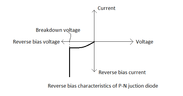
As can be seen from the characteristics plot, when reverse bias voltage is applied a very small reverse current flows which remains almost constant even with increasing reverse bias voltage up to a certain breakdown voltage. After the breakdown voltage, the reverse current increases by a large amount even for a small increase in the reverse voltage. This is because at breakdown voltage, the depletion layer breaks completely.
The breakdown can happen by two processes which are as follows:
(i) Avalanche breakdown – The minority charge carriers on both sides of the junction attain a lot of kinetic energy and thus, can knock out electrons from their covalent bonds, thus forming a large number of electron hole pairs and charge carriers. These charge carriers also get accelerated and flow to the other side thereby breaking down the depletion layer.
(ii) Zener breakdown – Zener diodes are special diodes which have a high level of doping and therefore, a thin depletion layer. This thin depletion layer gives rise to a large electric field which can pull out electrons from the minority side to the N-side, thereby resulting in a large reverse current and ultimate breakdown of the depletion layer. The breakdown in this case is called Zener breakdown and the breakdown voltage is called the Zener breakdown voltage.
Note: Students must remember that the reverse current in a P-N junction diode in reverse bias is much smaller in comparison to the forward current in forward bias, even when reverse breakdown is achieved. The reverse current is usually in microamperes, while forward currents can go up to thousands of amperes. Hence, in an experiment to plot the reverse bias characteristics of a P-N junction diode, a normal ammeter will not suffice to measure so small a current, but a micro ammeter has to be used.
Complete step by step answer:
During reverse bias, the P side of a P-N junction diode is connected to the negative terminal and the N-side to the positive terminal of a battery.
The reverse bias characteristics of a P-N junction diode are as follows.
As can be seen from the characteristics plot, when reverse bias voltage is applied a very small reverse current flows which remains almost constant even with increasing reverse bias voltage up to a certain breakdown voltage. After the breakdown voltage, the reverse current increases by a large amount even for a small increase in the reverse voltage. This is because at breakdown voltage, the depletion layer breaks completely.
The breakdown can happen by two processes which are as follows:
(i) Avalanche breakdown – The minority charge carriers on both sides of the junction attain a lot of kinetic energy and thus, can knock out electrons from their covalent bonds, thus forming a large number of electron hole pairs and charge carriers. These charge carriers also get accelerated and flow to the other side thereby breaking down the depletion layer.
(ii) Zener breakdown – Zener diodes are special diodes which have a high level of doping and therefore, a thin depletion layer. This thin depletion layer gives rise to a large electric field which can pull out electrons from the minority side to the N-side, thereby resulting in a large reverse current and ultimate breakdown of the depletion layer. The breakdown in this case is called Zener breakdown and the breakdown voltage is called the Zener breakdown voltage.
Note: Students must remember that the reverse current in a P-N junction diode in reverse bias is much smaller in comparison to the forward current in forward bias, even when reverse breakdown is achieved. The reverse current is usually in microamperes, while forward currents can go up to thousands of amperes. Hence, in an experiment to plot the reverse bias characteristics of a P-N junction diode, a normal ammeter will not suffice to measure so small a current, but a micro ammeter has to be used.
Recently Updated Pages
Master Class 12 Economics: Engaging Questions & Answers for Success
Master Class 12 Physics: Engaging Questions & Answers for Success
Master Class 12 English: Engaging Questions & Answers for Success
Master Class 12 Social Science: Engaging Questions & Answers for Success
Master Class 12 Maths: Engaging Questions & Answers for Success
Master Class 12 Business Studies: Engaging Questions & Answers for Success
Trending doubts
Which are the Top 10 Largest Countries of the World?
What are the major means of transport Explain each class 12 social science CBSE
Draw a labelled sketch of the human eye class 12 physics CBSE
Why cannot DNA pass through cell membranes class 12 biology CBSE
Differentiate between insitu conservation and exsitu class 12 biology CBSE
Draw a neat and well labeled diagram of TS of ovary class 12 biology CBSE