Draw the circuit arrangement for studying V-I characteristics of a P-N junction diode in reverse bias. Plot V-I characteristics in this case.
Answer
568.5k+ views
Hint: The P-N junction is reverse biased, that means the positive terminal of a voltage source is connected to the n-type region and the negative terminal of the source is connected to the p-type region. Cathode is at higher voltage than anode.
Complete step by step answer:
A P-N junction is a junction between two semiconductor devices, namely P and N type, inside a semiconductor. The P side is positive, and has an excess number of holes whereas the N type is negative having excess number of electrons.
In reverse biasing, the positive terminal of the battery is connected to N type and the negative terminal of the battery is connected to P type. In came of this biasing current flow is zero, this happens because cathode is made more positive with respect to anode.
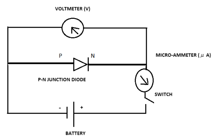
The circuit diagram for a PN Junction in reversed bias is as follows:

This circuit helps us in obtaining V-I characteristics in reverse bias.
When a P-N junction is reverse biased the negative terminal of the battery attracts the holes in P type towards itself and the positive terminal of the battery attracts the free electrons in N type towards itself. This results in creation of more positive impurity ions in the depletion layer which makes the layer of positive impurity ions thicker.
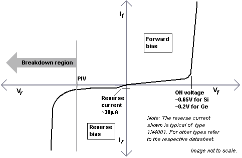
The V-I characteristics:

Here, voltage is taken along the X axis, and Current is taken along the Y axis.
In reverse bias, small or approximately no current flows.
Note: The maximum reverse voltage that can be applied to PN Junction is limited by Breakdown. Value of this voltage is referred to as breakdown voltage. In reverse bias, N side is held at a higher voltage than the P side.
Complete step by step answer:
A P-N junction is a junction between two semiconductor devices, namely P and N type, inside a semiconductor. The P side is positive, and has an excess number of holes whereas the N type is negative having excess number of electrons.
In reverse biasing, the positive terminal of the battery is connected to N type and the negative terminal of the battery is connected to P type. In came of this biasing current flow is zero, this happens because cathode is made more positive with respect to anode.
The circuit diagram for a PN Junction in reversed bias is as follows:

This circuit helps us in obtaining V-I characteristics in reverse bias.
When a P-N junction is reverse biased the negative terminal of the battery attracts the holes in P type towards itself and the positive terminal of the battery attracts the free electrons in N type towards itself. This results in creation of more positive impurity ions in the depletion layer which makes the layer of positive impurity ions thicker.
The V-I characteristics:

Here, voltage is taken along the X axis, and Current is taken along the Y axis.
In reverse bias, small or approximately no current flows.
Note: The maximum reverse voltage that can be applied to PN Junction is limited by Breakdown. Value of this voltage is referred to as breakdown voltage. In reverse bias, N side is held at a higher voltage than the P side.
Recently Updated Pages
Master Class 12 Economics: Engaging Questions & Answers for Success

Master Class 12 Physics: Engaging Questions & Answers for Success

Master Class 12 English: Engaging Questions & Answers for Success

Master Class 12 Social Science: Engaging Questions & Answers for Success

Master Class 12 Maths: Engaging Questions & Answers for Success

Master Class 12 Business Studies: Engaging Questions & Answers for Success

Trending doubts
Which are the Top 10 Largest Countries of the World?

What are the major means of transport Explain each class 12 social science CBSE

Draw a labelled sketch of the human eye class 12 physics CBSE

Why cannot DNA pass through cell membranes class 12 biology CBSE

Differentiate between insitu conservation and exsitu class 12 biology CBSE

Draw a neat and well labeled diagram of TS of ovary class 12 biology CBSE


