


Draw the circuit diagram of npn transistors in common emitter configuration. Hence, describe the working method to obtain the output characteristic curve.
Answer
564.6k+ views
Hint: The transistor consists of three regions: Emitter, Base and Collector. There are two parts of the circuit in the connection of a transistor. If the emitter region is common for both the parts, the transistor is said to be connected in the common-emitter transistor.
Complete step by step answer:
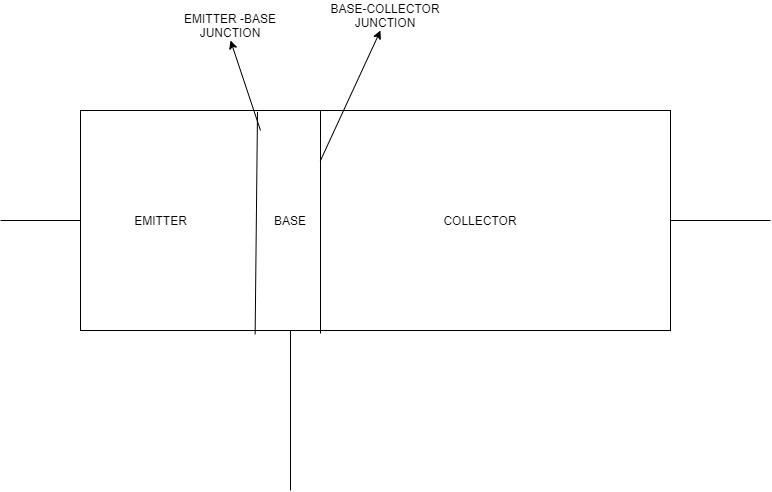
A transistor is a semiconductor device which is commonly used as a switch in electronic circuits and as an amplifier. It consists of three regions called Emitter, Base and Collector. The charge-carriers originate in the Emitter region and travel across the Base to the Collector region.
There are 2 P-N junctions: Emitter-Base junction and Base-Collector junction. The voltage applied to one junction causes changes in the other junction and is helpful in controlling it. Here is the schematic diagram of a transistor.
The transistor can be connected in three configurations with one of the three being in common. The three configurations are:
i) Common Emitter configuration
ii) Common Base configuration
iii) Common Collector configuration
The circuit diagram for Common Emitter configuration is given below –
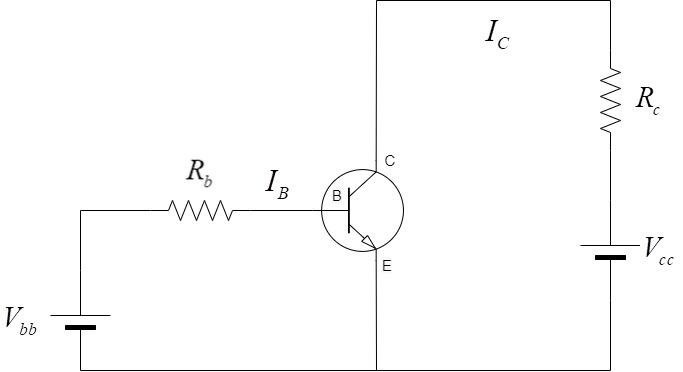
As per the above figure, the configuration in which the emitter is connected between the collector and base is known as a common emitter configuration. The input circuit is connected between emitter and base, and the output circuit is taken from the collector and emitter. Thus, the emitter is common to both the input and the output circuit.
Here, ${I_B}$ is the base-emitter current and ${I_C}$ is the collector-emitter current and the output voltage is given by –
${V_{CE}} = {V_{CC}} - {I_C}{R_C}$
Let us understand the working of the transistor in the CE configuration
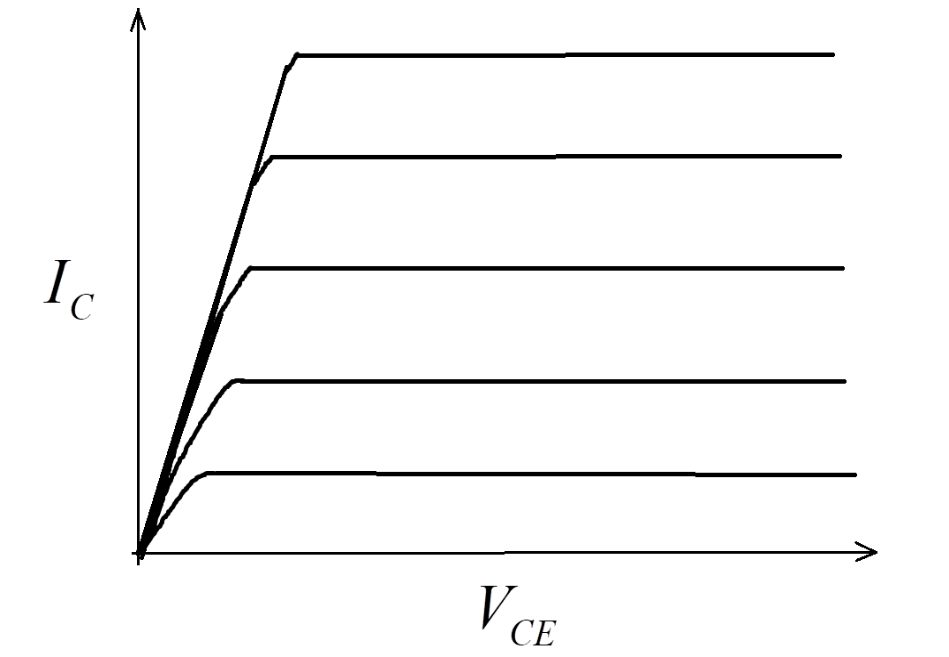
In common emitter configuration, the input current ${I_B}$ is very small, so it is measured in micro ampere , $\mu A$ .
The output voltage is given by, ${V_{CE}} = {V_{CC}} - {I_C}{R_C}$
If the out voltage ${V_{CE}}$ applied to the collector base junction is further increased, the depletion region width further increases.
The base region is lightly doped as compared to the collector region. So, the depletion region penetrates more into the base region and less into the collector region.
As a result, the width of the base region decreases in turn reducing the input current. And, it means that the output current or collector current, ${I_C}$ is larger as compared to the base current ${I_B}$ and so, it is measured in milli-ampere (mA).
As the output voltage increases from zero volt to different voltage level, since the cut in voltage is increased above 0.7 V so, in the active region the collector-emitter voltage or output voltage is measured in volts.
The output characteristics of CE configuration is the graph between output voltage ${V_{CE}}$ and collector current ${I_C}$. Here are the output characteristics for the CE configuration.
Note: The transistor connected in the CE configuration is used as a switch to transit between different states of the circuit and as an amplifier to increase the amplitude of the input signal by a certain constant. The other configurations of transistors such as CB and CC mode are rarely used.
Complete step by step answer:
A transistor is a semiconductor device which is commonly used as a switch in electronic circuits and as an amplifier. It consists of three regions called Emitter, Base and Collector. The charge-carriers originate in the Emitter region and travel across the Base to the Collector region.
There are 2 P-N junctions: Emitter-Base junction and Base-Collector junction. The voltage applied to one junction causes changes in the other junction and is helpful in controlling it. Here is the schematic diagram of a transistor.
The transistor can be connected in three configurations with one of the three being in common. The three configurations are:
i) Common Emitter configuration
ii) Common Base configuration
iii) Common Collector configuration
The circuit diagram for Common Emitter configuration is given below –
As per the above figure, the configuration in which the emitter is connected between the collector and base is known as a common emitter configuration. The input circuit is connected between emitter and base, and the output circuit is taken from the collector and emitter. Thus, the emitter is common to both the input and the output circuit.
Here, ${I_B}$ is the base-emitter current and ${I_C}$ is the collector-emitter current and the output voltage is given by –
${V_{CE}} = {V_{CC}} - {I_C}{R_C}$
Let us understand the working of the transistor in the CE configuration
In common emitter configuration, the input current ${I_B}$ is very small, so it is measured in micro ampere , $\mu A$ .
The output voltage is given by, ${V_{CE}} = {V_{CC}} - {I_C}{R_C}$
If the out voltage ${V_{CE}}$ applied to the collector base junction is further increased, the depletion region width further increases.
The base region is lightly doped as compared to the collector region. So, the depletion region penetrates more into the base region and less into the collector region.
As a result, the width of the base region decreases in turn reducing the input current. And, it means that the output current or collector current, ${I_C}$ is larger as compared to the base current ${I_B}$ and so, it is measured in milli-ampere (mA).
As the output voltage increases from zero volt to different voltage level, since the cut in voltage is increased above 0.7 V so, in the active region the collector-emitter voltage or output voltage is measured in volts.
The output characteristics of CE configuration is the graph between output voltage ${V_{CE}}$ and collector current ${I_C}$. Here are the output characteristics for the CE configuration.
Note: The transistor connected in the CE configuration is used as a switch to transit between different states of the circuit and as an amplifier to increase the amplitude of the input signal by a certain constant. The other configurations of transistors such as CB and CC mode are rarely used.
Recently Updated Pages
Master Class 12 Economics: Engaging Questions & Answers for Success
Master Class 12 Physics: Engaging Questions & Answers for Success
Master Class 12 English: Engaging Questions & Answers for Success
Master Class 12 Social Science: Engaging Questions & Answers for Success
Master Class 12 Maths: Engaging Questions & Answers for Success
Master Class 12 Business Studies: Engaging Questions & Answers for Success
Trending doubts
Which are the Top 10 Largest Countries of the World?
What are the major means of transport Explain each class 12 social science CBSE
Draw a labelled sketch of the human eye class 12 physics CBSE
Why cannot DNA pass through cell membranes class 12 biology CBSE
Differentiate between insitu conservation and exsitu class 12 biology CBSE
Draw a neat and well labeled diagram of TS of ovary class 12 biology CBSE