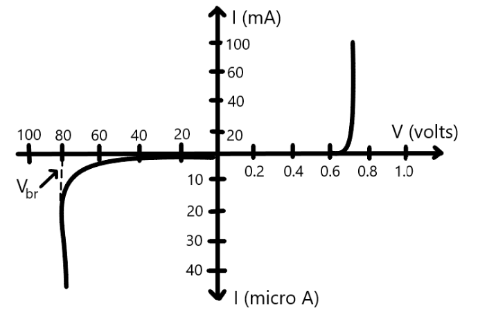
Draw V-I characteristics of a p-n junction diode. Explain why the current under reverse bias is almost independent of the applied voltage up to the critical voltage.
Answer
565.5k+ views
Hint: The V-I characteristics of a p-n junction diode can be used to find the relation between voltage and current. The relationship between the voltage and the current will be non-linear. The minority carriers in the junction will result in the current.
Complete answer:
The V-I characteristics of p-n junction diode represents the relation between current and voltage and the variations in current with respect to current is shown below;

Here, the X-axis represents the voltage or potential and the Y-axis represents the current in the p-n junction diode.
Now, when the p-n junction diode is reverse biased, the p-type of the semiconductor diode is connected to the negative terminal of the battery and the n-type of the semiconductor diode is connected to the positive terminal of the battery. Hence, the holes in the p-type of the semiconductor will be attracted by the negative terminal of the battery.
Also, the electrons in the n-type of the semiconductor will be attracted to the positive terminal of the battery. This results in barrier potential and hence, results in the increase of the depletion layer. As a result of this, the minority charge carrier will get drifted across the junction and result in the production of a small current.
Now, at the normal temperature, the current will be very low. Also, the applied voltage will provide very little change in the current which is almost negligible. Therefore, we can say that the current under reverse biased condition will be almost independent of the applied voltage.
Note:In the case of reverse biasing of the p-n junction diode, the built-in electric field and the applied electric field will be in the same direction. When we will add both the electric fields, the resultant electric field will be the same as that of the built-in electric field. This results in an increase in resistance in the diode and also an increase in the depletion layer of the diode.
Complete answer:
The V-I characteristics of p-n junction diode represents the relation between current and voltage and the variations in current with respect to current is shown below;

Here, the X-axis represents the voltage or potential and the Y-axis represents the current in the p-n junction diode.
Now, when the p-n junction diode is reverse biased, the p-type of the semiconductor diode is connected to the negative terminal of the battery and the n-type of the semiconductor diode is connected to the positive terminal of the battery. Hence, the holes in the p-type of the semiconductor will be attracted by the negative terminal of the battery.
Also, the electrons in the n-type of the semiconductor will be attracted to the positive terminal of the battery. This results in barrier potential and hence, results in the increase of the depletion layer. As a result of this, the minority charge carrier will get drifted across the junction and result in the production of a small current.
Now, at the normal temperature, the current will be very low. Also, the applied voltage will provide very little change in the current which is almost negligible. Therefore, we can say that the current under reverse biased condition will be almost independent of the applied voltage.
Note:In the case of reverse biasing of the p-n junction diode, the built-in electric field and the applied electric field will be in the same direction. When we will add both the electric fields, the resultant electric field will be the same as that of the built-in electric field. This results in an increase in resistance in the diode and also an increase in the depletion layer of the diode.
Recently Updated Pages
Master Class 12 Economics: Engaging Questions & Answers for Success

Master Class 12 Physics: Engaging Questions & Answers for Success

Master Class 12 English: Engaging Questions & Answers for Success

Master Class 12 Social Science: Engaging Questions & Answers for Success

Master Class 12 Maths: Engaging Questions & Answers for Success

Master Class 12 Business Studies: Engaging Questions & Answers for Success

Trending doubts
Which are the Top 10 Largest Countries of the World?

What are the major means of transport Explain each class 12 social science CBSE

Draw a labelled sketch of the human eye class 12 physics CBSE

Why cannot DNA pass through cell membranes class 12 biology CBSE

Differentiate between insitu conservation and exsitu class 12 biology CBSE

Draw a neat and well labeled diagram of TS of ovary class 12 biology CBSE


