


Explain how a potential barrier is developed in a p-n junction diode.
Answer
596.7k+ views
Hint:- First of all we will see the p-type semiconductor and n-type semiconductors and then and then the diode. The potential barrier in the P-N junction diode is the barrier in which additional force is required to cross the barrier.
Step By Step Answer:
As the semiconductor material of form P and N is put together, the gradient of very large density charge carriers is generated on both the side area P and N.
P-type semiconductors are those which have higher number of holes and these are formed by doping of semiconductors material with trivalent impurities like aluminum.
N-type is those which have higher numbers of free electrons and are formed with doping of pentavalent impurities like phosphorus with semiconductors.
The N-side free electrons traverse the area and continue to merge with the holes, leaving behind the immobile positive donor ions. Furthermore, the P-region holes fuse with the N-region electrons and leave behind the negative acceptor ions. The cycle is continued until there are enough charge carriers for the P and N regions to resist the corresponding electrons and holes.
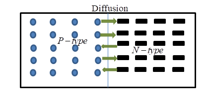
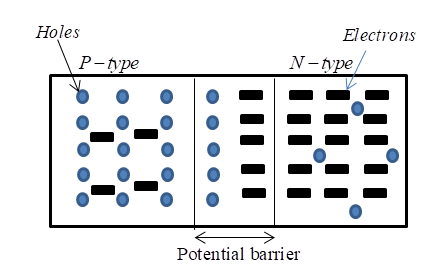
Thus when these electrons flow, positive charge leave behind and also holes leaving negative charge on its own side thus two different charge accumulate forming a layer as shown in figure known as depletion layer.
Note- As depletion layer is formed also now constitutes an electric field thus another form of current starts flowing due to this in the opposite direction of diffusion current and drift current. In unbiased condition these two current (diffusion and drift) are same and opposite in direction thus net current is zero.
Step By Step Answer:
As the semiconductor material of form P and N is put together, the gradient of very large density charge carriers is generated on both the side area P and N.
P-type semiconductors are those which have higher number of holes and these are formed by doping of semiconductors material with trivalent impurities like aluminum.
N-type is those which have higher numbers of free electrons and are formed with doping of pentavalent impurities like phosphorus with semiconductors.
The N-side free electrons traverse the area and continue to merge with the holes, leaving behind the immobile positive donor ions. Furthermore, the P-region holes fuse with the N-region electrons and leave behind the negative acceptor ions. The cycle is continued until there are enough charge carriers for the P and N regions to resist the corresponding electrons and holes.
Thus when these electrons flow, positive charge leave behind and also holes leaving negative charge on its own side thus two different charge accumulate forming a layer as shown in figure known as depletion layer.
Note- As depletion layer is formed also now constitutes an electric field thus another form of current starts flowing due to this in the opposite direction of diffusion current and drift current. In unbiased condition these two current (diffusion and drift) are same and opposite in direction thus net current is zero.
Recently Updated Pages
Master Class 12 Economics: Engaging Questions & Answers for Success
Master Class 12 Physics: Engaging Questions & Answers for Success
Master Class 12 English: Engaging Questions & Answers for Success
Master Class 12 Social Science: Engaging Questions & Answers for Success
Master Class 12 Maths: Engaging Questions & Answers for Success
Master Class 12 Business Studies: Engaging Questions & Answers for Success
Trending doubts
Which are the Top 10 Largest Countries of the World?
What are the major means of transport Explain each class 12 social science CBSE
Draw a labelled sketch of the human eye class 12 physics CBSE
Why cannot DNA pass through cell membranes class 12 biology CBSE
Differentiate between insitu conservation and exsitu class 12 biology CBSE
Draw a neat and well labeled diagram of TS of ovary class 12 biology CBSE