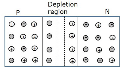
In the depletion region of an unbiased P-N junction diode there are
Answer
598.8k+ views
Hint: During the formation of the P-N junction diode, a thin layer is set up on both sides of the junction called depletion layer and it is devoid of free charge carriers. Its width is about 1μm. A barrier potential is also developed across the junction.
Complete step by step answer:
A P-N junction diode is a semiconductor material with one of its halves doped by P- type impurity and the other half is doped by N- type impurities. The division or junction between both the halves is called P-N junction. When P-N junction is formed, it has holes in P- region and electrons in N- region. The number of holes is higher in P- region (exists as majority carriers) than N- region (exists as minority carriers). In the same way, the quantity of electrons in N- region (exists as majority carriers) is higher than P- region (exists as minority carriers). The difference in density of carriers results in major carrier diffusion. So that, holes diffuse from P to N region and electrons diffuse from N to P region. The depletion layer is formed by the recombination of free or mobile holes and electrons that produce a narrow layer. And the region is depleted of free or mobile charge carriers. But it contains fixed and immobile charges. The production of ions is because of the impurity atoms that have let electrons and holes behind by themselves in an isolated state by having a charge that is opposite to the departed.

In the depletion region of an unbiased P-N junction diode there are only fixed or immobile positive and negative atoms.
Note: As the depletion layer contains no free or mobile charge carriers but only fixed and immobile ions, this layer (or region) behaves like an insulator. And due to the presence of rows of fixed and immobile charges, it possesses capacitance.
Complete step by step answer:
A P-N junction diode is a semiconductor material with one of its halves doped by P- type impurity and the other half is doped by N- type impurities. The division or junction between both the halves is called P-N junction. When P-N junction is formed, it has holes in P- region and electrons in N- region. The number of holes is higher in P- region (exists as majority carriers) than N- region (exists as minority carriers). In the same way, the quantity of electrons in N- region (exists as majority carriers) is higher than P- region (exists as minority carriers). The difference in density of carriers results in major carrier diffusion. So that, holes diffuse from P to N region and electrons diffuse from N to P region. The depletion layer is formed by the recombination of free or mobile holes and electrons that produce a narrow layer. And the region is depleted of free or mobile charge carriers. But it contains fixed and immobile charges. The production of ions is because of the impurity atoms that have let electrons and holes behind by themselves in an isolated state by having a charge that is opposite to the departed.

In the depletion region of an unbiased P-N junction diode there are only fixed or immobile positive and negative atoms.
Note: As the depletion layer contains no free or mobile charge carriers but only fixed and immobile ions, this layer (or region) behaves like an insulator. And due to the presence of rows of fixed and immobile charges, it possesses capacitance.
Recently Updated Pages
Master Class 12 Economics: Engaging Questions & Answers for Success

Master Class 12 Physics: Engaging Questions & Answers for Success

Master Class 12 English: Engaging Questions & Answers for Success

Master Class 12 Social Science: Engaging Questions & Answers for Success

Master Class 12 Maths: Engaging Questions & Answers for Success

Master Class 12 Business Studies: Engaging Questions & Answers for Success

Trending doubts
Which are the Top 10 Largest Countries of the World?

What are the major means of transport Explain each class 12 social science CBSE

Draw a labelled sketch of the human eye class 12 physics CBSE

Why cannot DNA pass through cell membranes class 12 biology CBSE

Differentiate between insitu conservation and exsitu class 12 biology CBSE

Draw a neat and well labeled diagram of TS of ovary class 12 biology CBSE


