
How will you obtain OR, AND gates from the NAND and NOR gates? Write symbols, Boolean formula, and truth table.
Answer
543.6k+ views
Hint: When we join the inputs of a NAND gate we can obtain a NOT gate. Also, when joining the two inputs of a NOR gate together we can obtain a NOT gate.
Formula used: In this solution we will be using the following formula;
\[NOT(A) = \overline A \] where \[A\] is an input.
\[OR(AB) = A + B\], \[OR\] signifies the OR gates acting on input A and B,
\[AND(AB) = A \cdot B\], AND signifies the AND gates acting on input A and B
Complete answer:
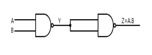
To obtain an AND gate from NAND gates, we first feed the inputs A and B into the NAND gates.
When, the output says Y is fed into another NAND gate with the two inputs joined together to obtain an output, say Z which is NOT (NAND Y). This is because joining the input of a NAND gate will give a NOT gate.
Boolean formula: \[Z = \overline Y = \overline{\overline {A \cdot B}} = A \cdot B\],
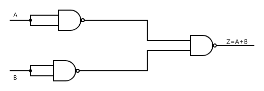
To obtain OR gate from NAND gates, we feed input A into a NAND with the input joined together to obtain a NOT (A), we feed input B into another NAND gate NAND with the input joined together to obtain NOT (B). Now the NOT (A) and NOT (B) are fed into separate input of another NAND gate. Hence, it becomes a NAND(NOT(A) NOT (B)) or \[NAND\left( {\overline A \overline B } \right)\] which is equal to the OR gate.
Boolean formula: \[Z = \overline {{Y_1} \cdot {Y_2}} = \overline {\overline A \cdot \overline B } = \overline{\overline A} + \overline{\overline B} = A + B\]
To obtain an OR gate from NOR gates, the input A and B is fed into a NOR gate (into the separate inputs), then the output say Y which is NOT(A or B) is fed into two another NOR gates with the inputs combined to have a NOT (NOR Y) which is an OR gate.
Boolean formula: \[Z = \overline Y = \overline{\overline {A + B}} = A + B\]

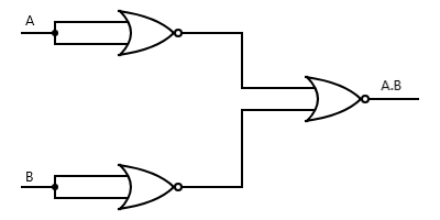
To obtain an AND gate from NOR gates, we feed input A and B into two separate NOR gates with joined input to obtain a NOT (A) and a NOT (B) separately. Then this two different outputs are fed into either input (i.e. NOT (A) to one Input terminal and NOT (B) to another terminal). The result will be an AND gate.
Boolean formula: \[Z = NOR\left( {\overline A \overline B } \right) = \overline {\overline A + \overline B } = \overline{\overline A} \cdot \overline{\overline B} = A \cdot B\]
Note:
For clarity, joining the inputs of NAND and NOR gate gives us NOT gate because AND and OR act necessarily on two inputs. Hence, when the inputs NAND (or NOR) are joined to allow only one input, it opens the AND (or OR) circuit and acts as NOT circuit, since NAND actually means NOT-AND and NOR means NOT-OR. So when the AND and NOR are removed it becomes a NOT.
Formula used: In this solution we will be using the following formula;
\[NOT(A) = \overline A \] where \[A\] is an input.
\[OR(AB) = A + B\], \[OR\] signifies the OR gates acting on input A and B,
\[AND(AB) = A \cdot B\], AND signifies the AND gates acting on input A and B
Complete answer:
To obtain an AND gate from NAND gates, we first feed the inputs A and B into the NAND gates.
When, the output says Y is fed into another NAND gate with the two inputs joined together to obtain an output, say Z which is NOT (NAND Y). This is because joining the input of a NAND gate will give a NOT gate.
Boolean formula: \[Z = \overline Y = \overline{\overline {A \cdot B}} = A \cdot B\],
| A | B | Y | Z |
| 0 | 0 | 1 | 0 |
| 1 | 0 | 1 | 0 |
| 0 | 1 | 1 | 0 |
| 1 | 0 | 0 | 1 |

To obtain OR gate from NAND gates, we feed input A into a NAND with the input joined together to obtain a NOT (A), we feed input B into another NAND gate NAND with the input joined together to obtain NOT (B). Now the NOT (A) and NOT (B) are fed into separate input of another NAND gate. Hence, it becomes a NAND(NOT(A) NOT (B)) or \[NAND\left( {\overline A \overline B } \right)\] which is equal to the OR gate.
Boolean formula: \[Z = \overline {{Y_1} \cdot {Y_2}} = \overline {\overline A \cdot \overline B } = \overline{\overline A} + \overline{\overline B} = A + B\]
| A | B | \[{Y_1}\] | \[{Y_2}\] | \[Z\] |
| 0 | 0 | 1 | 1 | 0 |
| 1 | 0 | 0 | 1 | 1 |
| 0 | 1 | 1 | 0 | 1 |
| 1 | 1 | 0 | 0 | 1 |

To obtain an OR gate from NOR gates, the input A and B is fed into a NOR gate (into the separate inputs), then the output say Y which is NOT(A or B) is fed into two another NOR gates with the inputs combined to have a NOT (NOR Y) which is an OR gate.
Boolean formula: \[Z = \overline Y = \overline{\overline {A + B}} = A + B\]
| A | B | Y | Z |
| 0 | 0 | 1 | 0 |
| 0 | 1 | 0 | 1 |
| 1 | 0 | 0 | 1 |
| 1 | 1 | 0 | 1 |

To obtain an AND gate from NOR gates, we feed input A and B into two separate NOR gates with joined input to obtain a NOT (A) and a NOT (B) separately. Then this two different outputs are fed into either input (i.e. NOT (A) to one Input terminal and NOT (B) to another terminal). The result will be an AND gate.
Boolean formula: \[Z = NOR\left( {\overline A \overline B } \right) = \overline {\overline A + \overline B } = \overline{\overline A} \cdot \overline{\overline B} = A \cdot B\]
| A | B | \[\overline A \] | \[\overline B \] | Z |
| 0 | 0 | 1 | 1 | 0 |
| 0 | 1 | 1 | 0 | 0 |
| 1 | 0 | 0 | 1 | 0 |
| 1 | 1 | 0 | 0 | 1 |

Note:
For clarity, joining the inputs of NAND and NOR gate gives us NOT gate because AND and OR act necessarily on two inputs. Hence, when the inputs NAND (or NOR) are joined to allow only one input, it opens the AND (or OR) circuit and acts as NOT circuit, since NAND actually means NOT-AND and NOR means NOT-OR. So when the AND and NOR are removed it becomes a NOT.
Recently Updated Pages
Master Class 12 Economics: Engaging Questions & Answers for Success

Master Class 12 Physics: Engaging Questions & Answers for Success

Master Class 12 English: Engaging Questions & Answers for Success

Master Class 12 Social Science: Engaging Questions & Answers for Success

Master Class 12 Maths: Engaging Questions & Answers for Success

Master Class 12 Business Studies: Engaging Questions & Answers for Success

Trending doubts
Which are the Top 10 Largest Countries of the World?

What are the major means of transport Explain each class 12 social science CBSE

Draw a labelled sketch of the human eye class 12 physics CBSE

Why cannot DNA pass through cell membranes class 12 biology CBSE

Differentiate between insitu conservation and exsitu class 12 biology CBSE

Draw a neat and well labeled diagram of TS of ovary class 12 biology CBSE


