


The Fermi level in intrinsic semiconductor at $0K$ temperature lies:
A. Near the conduction band
B. Near the valence band
C. In the middle of the valence and conduction band
D. inside the conduction band
Answer
595.5k+ views
Hint: First, we know that a semiconductor is defined as whose conductivity and resistivity lie between conductor and insulator. They are of two types, i.e. intrinsic and extrinsic semiconductors. Intrinsic semiconductors are pure semiconductor or undoped semiconductor without any significant dopant, and extrinsic semiconductor is an impure semiconductor having significant dopant.
Complete step by step answer:
In an intrinsic semiconductor, the number of holes in the valence band is equal to the number of electrons in the conduction band. Hence the probability of occupation of energy levels in the conduction band and valence band are equal. Thus the Fermi level for the intrinsic semiconductor lies in the middle of the forbidden band.
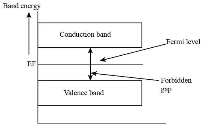
At $0K$, the intrinsic semiconductor acts as a perfect insulator.
Additional information: Fermi level changes with temperature, when the temperature rises, electrons acquire energy and move from lower energy level to higher energy level. So the Fermi level changed. The same kind of reaction will have occurred between the electrons and holes during doping in semiconductors. Fermi level in n-type semiconductor lies near the conduction band or in p-type semiconductor lies near in the valence band.
Note: Exactly the Fermi level of a solid-state body is a thermodynamic work required to add one electron of the body. It is denoted by ${E_F}$. The Fermi level does not include the work required to remove the electron whenever it came from.
Complete step by step answer:
In an intrinsic semiconductor, the number of holes in the valence band is equal to the number of electrons in the conduction band. Hence the probability of occupation of energy levels in the conduction band and valence band are equal. Thus the Fermi level for the intrinsic semiconductor lies in the middle of the forbidden band.
At $0K$, the intrinsic semiconductor acts as a perfect insulator.
Additional information: Fermi level changes with temperature, when the temperature rises, electrons acquire energy and move from lower energy level to higher energy level. So the Fermi level changed. The same kind of reaction will have occurred between the electrons and holes during doping in semiconductors. Fermi level in n-type semiconductor lies near the conduction band or in p-type semiconductor lies near in the valence band.
Note: Exactly the Fermi level of a solid-state body is a thermodynamic work required to add one electron of the body. It is denoted by ${E_F}$. The Fermi level does not include the work required to remove the electron whenever it came from.
Recently Updated Pages
Master Class 12 Economics: Engaging Questions & Answers for Success
Master Class 12 Physics: Engaging Questions & Answers for Success
Master Class 12 English: Engaging Questions & Answers for Success
Master Class 12 Social Science: Engaging Questions & Answers for Success
Master Class 12 Maths: Engaging Questions & Answers for Success
Master Class 12 Business Studies: Engaging Questions & Answers for Success
Trending doubts
Which are the Top 10 Largest Countries of the World?
What are the major means of transport Explain each class 12 social science CBSE
Draw a labelled sketch of the human eye class 12 physics CBSE
Why cannot DNA pass through cell membranes class 12 biology CBSE
Differentiate between insitu conservation and exsitu class 12 biology CBSE
Draw a neat and well labeled diagram of TS of ovary class 12 biology CBSE