


The ratio of forward bias to reverse bias resistance of p-n junction diode is:
$\begin{gathered}
{\text{A}}{\text{. 1}}{{\text{0}}^{ - 1}}:1 \\
{\text{B}}{\text{. 1}}{{\text{0}}^{ - 2}}:1 \\
{\text{C}}{\text{. 1}}{{\text{0}}^{ - 3}}:1 \\
{\text{D}}{\text{. 1}}{{\text{0}}^{ - 4}}:1 \\
\end{gathered} $
Answer
597k+ views
Hint: When diode is forward biased the thickness of the depletion decreases , thereby increasing the current in the circuit while during reverse biasing the thickness of depletion layer increases, reducing the current in circuit.
Complete step-by-step answer:
A p-n junction is an electronic semiconductor device which consists of a p-type semiconductor joined with a n-type semiconductor. The region where these semiconductors are joined with each other is called the depletion region. In this region, the holes from the p-side recombine with electrons from the n-side creating a region of neutrality also called space charge region.
This device has two terminals and there are two ways of connecting positive and negative terminals of the battery to the diode.
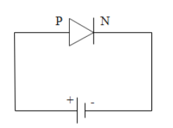
When the positive terminal of the battery is joined to the p-side of the p-n junction then it is called forward biasing of the p-n junction diode. In this configuration, the holes from the p-side move towards the negative terminal of the battery while electrons from the n-side move towards the positive terminal of the battery crossing the depletion layer. The thickness of the depletion layer reduces because space charges break apart due to the flow of current.
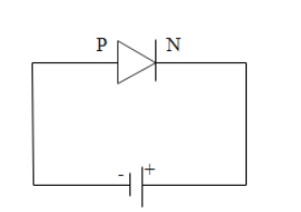
When the positive terminal of the battery is joined to the n-side of the p-n junction then it is called reverse biasing of the p-n junction diode. In this configuration, the charge carriers move away from the depletion layer. The thickness of the depletion layer increases and conductivity decreases.
When we compare the conductivity in forward and reverse biasing, the resistance to flow of current is very large in case of reverse biasing. For silicon diodes, the ratio of forward resistance to reverse resistance is ${10^{ - 5}}:1$ while for germanium diodes, the ratio is ${10^{ - 4}}:1$.
Hence the correct answer is option D.
Note: The small amount of current is possible in case of reverse biasing due to the presence of minority charge carriers on either side of the diode. But the value of applied reverse voltage leads to the breakdown of the diode.
Complete step-by-step answer:
A p-n junction is an electronic semiconductor device which consists of a p-type semiconductor joined with a n-type semiconductor. The region where these semiconductors are joined with each other is called the depletion region. In this region, the holes from the p-side recombine with electrons from the n-side creating a region of neutrality also called space charge region.
This device has two terminals and there are two ways of connecting positive and negative terminals of the battery to the diode.
When the positive terminal of the battery is joined to the p-side of the p-n junction then it is called forward biasing of the p-n junction diode. In this configuration, the holes from the p-side move towards the negative terminal of the battery while electrons from the n-side move towards the positive terminal of the battery crossing the depletion layer. The thickness of the depletion layer reduces because space charges break apart due to the flow of current.
When the positive terminal of the battery is joined to the n-side of the p-n junction then it is called reverse biasing of the p-n junction diode. In this configuration, the charge carriers move away from the depletion layer. The thickness of the depletion layer increases and conductivity decreases.
When we compare the conductivity in forward and reverse biasing, the resistance to flow of current is very large in case of reverse biasing. For silicon diodes, the ratio of forward resistance to reverse resistance is ${10^{ - 5}}:1$ while for germanium diodes, the ratio is ${10^{ - 4}}:1$.
Hence the correct answer is option D.
Note: The small amount of current is possible in case of reverse biasing due to the presence of minority charge carriers on either side of the diode. But the value of applied reverse voltage leads to the breakdown of the diode.
Recently Updated Pages
Master Class 12 Economics: Engaging Questions & Answers for Success
Master Class 12 Physics: Engaging Questions & Answers for Success
Master Class 12 English: Engaging Questions & Answers for Success
Master Class 12 Social Science: Engaging Questions & Answers for Success
Master Class 12 Maths: Engaging Questions & Answers for Success
Master Class 12 Business Studies: Engaging Questions & Answers for Success
Trending doubts
Why cannot DNA pass through cell membranes class 12 biology CBSE
Differentiate between insitu conservation and exsitu class 12 biology CBSE
Draw a neat and well labeled diagram of TS of ovary class 12 biology CBSE
In a human foetus the limbs and digits develop after class 12 biology CBSE
AABbCc genotype forms how many types of gametes a 4 class 12 biology CBSE
The correct structure of ethylenediaminetetraacetic class 12 chemistry CBSE