


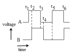
The waveforms A and B given below are given as input to a NAND gate. Then, its logic output is y is
A.)For ${t_1}$ to ${t_2}$; $y = 0$
B.)For ${t_2}$ to ${t_3}$; $y = 1$
C.)For ${t_3}$ to ${t_4}$; $y = 1$
D.)For ${t_4}$ to ${t_5}$; $y = 0$
E.)For ${t_5}$ to ${t_6}$; $y = 0$
Answer
600.6k+ views
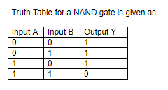
Hint: NAND gate is the combination of a NOT gate and a AND gate. The property of AND is that its output is equal to the product of the input while the NOT gate gives output opposite to the input fed to it.
Detailed step by step answer:
A NAND gate is made by connecting a NOT gate and a AND gate with each other. The symbol for NAND gate is given as
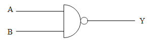
The Boolean expression for a NAND gate is given as
$Y = \mathop {A.B}\limits^{\_\_\_\_\_\_} = \mathop A\limits^{\_\_} + \mathop B\limits^{\_\_} $
For ${t_1}$ to ${t_2}$; we have A = 1 and B = 0, using the Boolean algebra or the truth table for NAND gate we get y = 1
For ${t_2}$ to ${t_3}$; we have A = 1 and B = 1, using the Boolean algebra or the truth table for NAND gate we get y = 0
For ${t_3}$ to ${t_4}$; we have A = 0 and B = 1, using the Boolean algebra or the truth table for NAND gate we get y = 1
For ${t_4}$ to ${t_5}$; we have A = 0 and B = 0, using the Boolean algebra or the truth table for NAND gate we get y = 1
For ${t_5}$ to ${t_6}$; we have A = 1 and B = 0, using the Boolean algebra or the truth table for NAND gate we get y = 1
On the basis of the above results, the correct option is C from the given choices.
Note:
1. In digital electronics, the higher value of voltage is considered 1 whereas lower value of voltage is considered 0.
2. In order to obtain a NAND gate, the AND and NOT gate must be connected in series with each other. Attaching them in parallel will not give the desired gate.
Detailed step by step answer:
A NAND gate is made by connecting a NOT gate and a AND gate with each other. The symbol for NAND gate is given as
The Boolean expression for a NAND gate is given as
$Y = \mathop {A.B}\limits^{\_\_\_\_\_\_} = \mathop A\limits^{\_\_} + \mathop B\limits^{\_\_} $
For ${t_1}$ to ${t_2}$; we have A = 1 and B = 0, using the Boolean algebra or the truth table for NAND gate we get y = 1
For ${t_2}$ to ${t_3}$; we have A = 1 and B = 1, using the Boolean algebra or the truth table for NAND gate we get y = 0
For ${t_3}$ to ${t_4}$; we have A = 0 and B = 1, using the Boolean algebra or the truth table for NAND gate we get y = 1
For ${t_4}$ to ${t_5}$; we have A = 0 and B = 0, using the Boolean algebra or the truth table for NAND gate we get y = 1
For ${t_5}$ to ${t_6}$; we have A = 1 and B = 0, using the Boolean algebra or the truth table for NAND gate we get y = 1
On the basis of the above results, the correct option is C from the given choices.
Note:
1. In digital electronics, the higher value of voltage is considered 1 whereas lower value of voltage is considered 0.
2. In order to obtain a NAND gate, the AND and NOT gate must be connected in series with each other. Attaching them in parallel will not give the desired gate.
Recently Updated Pages
Master Class 12 Economics: Engaging Questions & Answers for Success
Master Class 12 Physics: Engaging Questions & Answers for Success
Master Class 12 English: Engaging Questions & Answers for Success
Master Class 12 Social Science: Engaging Questions & Answers for Success
Master Class 12 Maths: Engaging Questions & Answers for Success
Master Class 12 Business Studies: Engaging Questions & Answers for Success
Trending doubts
Which are the Top 10 Largest Countries of the World?
What are the major means of transport Explain each class 12 social science CBSE
Draw a labelled sketch of the human eye class 12 physics CBSE
Why cannot DNA pass through cell membranes class 12 biology CBSE
Differentiate between insitu conservation and exsitu class 12 biology CBSE
Draw a neat and well labeled diagram of TS of ovary class 12 biology CBSE