


With the help of circuit diagram, explain the V-I characteristics of p-n junction diodes in forward biasing.
Answer
574.2k+ views
Hint: We know that a p-n junction diode is a solid substance that has the value of conductivity just between the insulator and most of the metal it is actually a semiconductor, we also know that this feature of the diode is due to added impurities in the semiconductor material that the value of conductivity is like this. VI characteristics graph is the graph that gives us an idea about voltage and current relationship in a semiconductor.
Complete step by step answer:
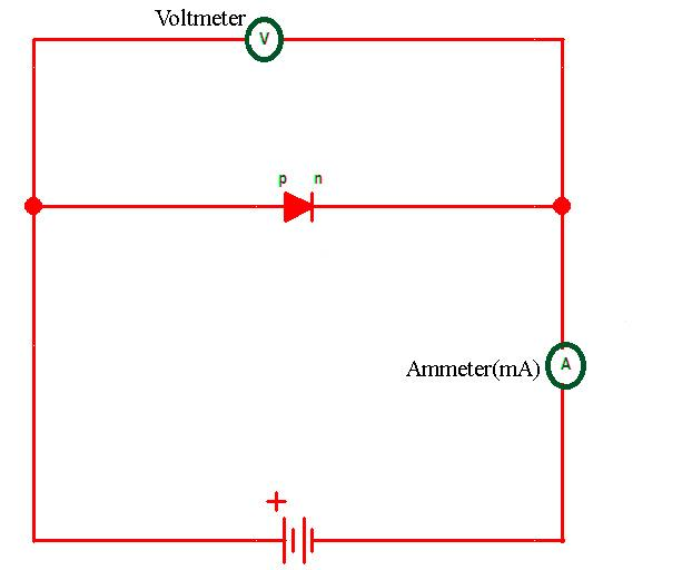
Here in the diagram we can see a circuit and this circuit is the forward biased circuit for the p-n junction diode. Here we see one ammeter, one voltmeter and also a battery.
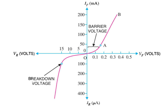
In the graph that is given above we see that when the graph reaches certain points, that is when the current is 100 mA approximately and the voltage 15 V approximately then we can see that it reaches the breakdown voltage and after that, there is a rapid change in VI characteristics. On the other side, we can see that the same happens when it reaches barrier voltage after reaching the barrier voltage it suddenly gives a rapid change to the VI characteristics.
So, we can say by seeing the graph that the VI characteristics of PN junction diodes are nonlinear in forwarding bias, that is, it is not a straight line. Now, this nonlinear characteristic generally illustrates that during the N junction is operated the resistance is variable or not a constant value. Now further we can see that the slope of the PN junction diode in forwarding bias depicts that the resistance is very low. When we apply a forward bias to the diode then it gives a low impedance path and permits the circuit which conducts a large amount of current which we call infinite current. Usually this current has low amount of external potential and flows above the knee point. The potential difference across the PN junction of the pn junction diode is maintained constant by the depletion of the layer action. The maximum amount of current that has to be conducted is generally kept incomplete by the load resistance because when the PN junction diode conducts more current than the normal amount of current that it draws, then the extra current results in the heat dissipation and also leads to damaging of the device.
Note: Minute details to be covered while reading this part of the chapter, sometimes students confuse between reverse biased and forward biased. They also confuse the concept of electrons exchange. Students should remember that the reverse current is independent of critical voltage.
Complete step by step answer:
Here in the diagram we can see a circuit and this circuit is the forward biased circuit for the p-n junction diode. Here we see one ammeter, one voltmeter and also a battery.
In the graph that is given above we see that when the graph reaches certain points, that is when the current is 100 mA approximately and the voltage 15 V approximately then we can see that it reaches the breakdown voltage and after that, there is a rapid change in VI characteristics. On the other side, we can see that the same happens when it reaches barrier voltage after reaching the barrier voltage it suddenly gives a rapid change to the VI characteristics.
So, we can say by seeing the graph that the VI characteristics of PN junction diodes are nonlinear in forwarding bias, that is, it is not a straight line. Now, this nonlinear characteristic generally illustrates that during the N junction is operated the resistance is variable or not a constant value. Now further we can see that the slope of the PN junction diode in forwarding bias depicts that the resistance is very low. When we apply a forward bias to the diode then it gives a low impedance path and permits the circuit which conducts a large amount of current which we call infinite current. Usually this current has low amount of external potential and flows above the knee point. The potential difference across the PN junction of the pn junction diode is maintained constant by the depletion of the layer action. The maximum amount of current that has to be conducted is generally kept incomplete by the load resistance because when the PN junction diode conducts more current than the normal amount of current that it draws, then the extra current results in the heat dissipation and also leads to damaging of the device.
Note: Minute details to be covered while reading this part of the chapter, sometimes students confuse between reverse biased and forward biased. They also confuse the concept of electrons exchange. Students should remember that the reverse current is independent of critical voltage.
Recently Updated Pages
Master Class 12 Economics: Engaging Questions & Answers for Success
Master Class 12 Physics: Engaging Questions & Answers for Success
Master Class 12 English: Engaging Questions & Answers for Success
Master Class 12 Social Science: Engaging Questions & Answers for Success
Master Class 12 Maths: Engaging Questions & Answers for Success
Master Class 12 Business Studies: Engaging Questions & Answers for Success
Trending doubts
Which are the Top 10 Largest Countries of the World?
What are the major means of transport Explain each class 12 social science CBSE
Draw a labelled sketch of the human eye class 12 physics CBSE
Why cannot DNA pass through cell membranes class 12 biology CBSE
Differentiate between insitu conservation and exsitu class 12 biology CBSE
Draw a neat and well labeled diagram of TS of ovary class 12 biology CBSE