How will the forbidden energy band gap of a semiconductor vary with temperature?
(A). Increases with increase in temperature.
(B). Decrease with the increase in temperature.
(C). First increase, then decrease with increase in temperature.
(D). No variation due to increase in temperature.
Answer
526.1k+ views
- Hint: The term gap in a general sense means there is a space which is empty between two regions. Here we are talking about the energy gap. We must have a clear idea about how temperature enables electrons from a lower energy level to get to higher energy levels.
Complete step-by-step solution -
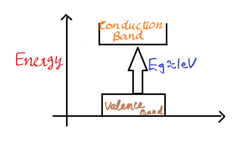
First, we need to understand what is a forbidden energy gap. The forbidden energy band gap of a semiconductor is the energy difference (in eV) between the top of the conduction band and the bottom of the valence band in any materials whether it be a metal, an insulator or a semiconductor.
For easy understanding, we can say that the gap is a region where there are no states available for an electron to occupy.
In semiconductors, the conduction band and the valence band are separated by a small energy difference of about 1 eV. This is a small energy difference and can be overcome by thermal agitation.

The energy gap of a semiconductor material is dependent on the temperature. So as the temperature increases from room temperature there is a decrease in the forbidden energy gap. The relation between the forbidden energy gap and temperature is given by the equation,
$E_{g}(T)=E_{g}(0)-\dfrac{\alpha T^{2}}{T+\beta}$
Where,
$E_{g}(T)$ is the forbidden energy gap of the semiconductor at a temperature T.
$E_{g}(0)$ is the intrinsic forbidden energy gap of the semiconductor.
$\alpha$ and $\beta$ are constants.
Hence, Option (B) is correct.
Note: In the case of metals, the conduction band and valence band overlap each other. In insulators, the conduction band and the valence band are separated by a high energy difference (greater than 10 eV).
Complete step-by-step solution -
First, we need to understand what is a forbidden energy gap. The forbidden energy band gap of a semiconductor is the energy difference (in eV) between the top of the conduction band and the bottom of the valence band in any materials whether it be a metal, an insulator or a semiconductor.
For easy understanding, we can say that the gap is a region where there are no states available for an electron to occupy.
In semiconductors, the conduction band and the valence band are separated by a small energy difference of about 1 eV. This is a small energy difference and can be overcome by thermal agitation.

The energy gap of a semiconductor material is dependent on the temperature. So as the temperature increases from room temperature there is a decrease in the forbidden energy gap. The relation between the forbidden energy gap and temperature is given by the equation,
$E_{g}(T)=E_{g}(0)-\dfrac{\alpha T^{2}}{T+\beta}$
Where,
$E_{g}(T)$ is the forbidden energy gap of the semiconductor at a temperature T.
$E_{g}(0)$ is the intrinsic forbidden energy gap of the semiconductor.
$\alpha$ and $\beta$ are constants.
Hence, Option (B) is correct.
Note: In the case of metals, the conduction band and valence band overlap each other. In insulators, the conduction band and the valence band are separated by a high energy difference (greater than 10 eV).
Recently Updated Pages
Master Class 12 Economics: Engaging Questions & Answers for Success

Master Class 12 Physics: Engaging Questions & Answers for Success

Master Class 12 English: Engaging Questions & Answers for Success

Master Class 12 Social Science: Engaging Questions & Answers for Success

Master Class 12 Maths: Engaging Questions & Answers for Success

Master Class 12 Business Studies: Engaging Questions & Answers for Success

Trending doubts
Which are the Top 10 Largest Countries of the World?

What are the major means of transport Explain each class 12 social science CBSE

Draw a labelled sketch of the human eye class 12 physics CBSE

Why cannot DNA pass through cell membranes class 12 biology CBSE

Differentiate between insitu conservation and exsitu class 12 biology CBSE

Draw a neat and well labeled diagram of TS of ovary class 12 biology CBSE


