


The n-side of the depletion layer of a p-n junction.
\[A.\] Always has the same width as the p-side.
\[B.\] Has no bound charges
\[C.\] Is negatively charged.
\[D.\] Is positively charged.
Answer
595.8k+ views
Hint: We will look at the components of \[p-side\] and \[n-side\] of a p-n junction diode and also about the minority charge carriers. The depletion region is formed by the majority charge carried of the particular side. We can then see the charge at the depletion layer of a particular side.
Complete solution: First of all let us understand the majority and minority charge carriers in \[N-type\] and \[P-type\] semiconductors. In \[N-type\] they have excess free electrons compared to\[P-type\]which have excess holes. So, the minority carriers in both will be holes and electrons respectively.
Now, if we look at how a depletion layer is formed in p-n junction diodes which are formed by combining an \[N-type\] and a \[P-type\] semiconductor, electrons and holes diffuse into regions with lower concentration. Therefore, free electrons from \[n-side\] diffuse into \[p-side\] and holes from \[p-side\] diffuses into \[n-side\].
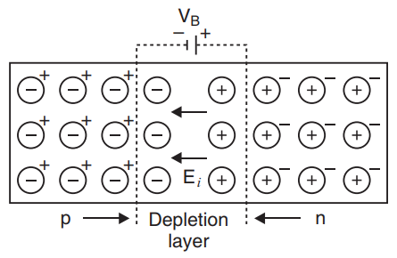
Now, at the \[n-side\] region near the junction, the free electrons are gone by the diffusion of electrons to \[p-side\] and recombination of electrons to holes that are diffused from\[p-side\]. Similarly, the holes from \[p-side\] will also be gone. As a result, majority charge carriers are depleted at the junction which is called a depletion layer.
Due to this depletion layer, both the sides will be charged as, \[n-side\] will be positively charged and \[p-side\] will be negatively charged. Therefore, option d is the correct answer.
Note: We must be aware of the fact that the charges at the depletion layer are non-mobile charges and they act like a barrier that opposes the flow of electrons and holes. The width of this layer will change according to the biasing conditions and hence the potential difference will change. That means the charge at either side will differ.
Complete solution: First of all let us understand the majority and minority charge carriers in \[N-type\] and \[P-type\] semiconductors. In \[N-type\] they have excess free electrons compared to\[P-type\]which have excess holes. So, the minority carriers in both will be holes and electrons respectively.
Now, if we look at how a depletion layer is formed in p-n junction diodes which are formed by combining an \[N-type\] and a \[P-type\] semiconductor, electrons and holes diffuse into regions with lower concentration. Therefore, free electrons from \[n-side\] diffuse into \[p-side\] and holes from \[p-side\] diffuses into \[n-side\].
Now, at the \[n-side\] region near the junction, the free electrons are gone by the diffusion of electrons to \[p-side\] and recombination of electrons to holes that are diffused from\[p-side\]. Similarly, the holes from \[p-side\] will also be gone. As a result, majority charge carriers are depleted at the junction which is called a depletion layer.
Due to this depletion layer, both the sides will be charged as, \[n-side\] will be positively charged and \[p-side\] will be negatively charged. Therefore, option d is the correct answer.
Note: We must be aware of the fact that the charges at the depletion layer are non-mobile charges and they act like a barrier that opposes the flow of electrons and holes. The width of this layer will change according to the biasing conditions and hence the potential difference will change. That means the charge at either side will differ.
Recently Updated Pages
Master Class 12 Economics: Engaging Questions & Answers for Success
Master Class 12 Physics: Engaging Questions & Answers for Success
Master Class 12 English: Engaging Questions & Answers for Success
Master Class 12 Social Science: Engaging Questions & Answers for Success
Master Class 12 Maths: Engaging Questions & Answers for Success
Master Class 12 Business Studies: Engaging Questions & Answers for Success
Trending doubts
Which are the Top 10 Largest Countries of the World?
What are the major means of transport Explain each class 12 social science CBSE
Draw a labelled sketch of the human eye class 12 physics CBSE
What is a transformer Explain the principle construction class 12 physics CBSE
Why cannot DNA pass through cell membranes class 12 biology CBSE
Differentiate between insitu conservation and exsitu class 12 biology CBSE