


What is the order of forbidden gaps in the energy bands of silicon?
Answer
493.2k+ views
Hint: The term gap normally implies the vacant space where there is nothing. But here we are talking about the energy band gap. Forbidden energy gap is defined as the difference of energy levels of conduction band and valence band.
Complete answer:
Forbidden energy gap is defined as the difference of energy from the conduction band to the valence band. In other words, it can be said that the energy that an electron requires to escape from the valence band to the conduction band is known as the forbidden energy gap.It’s SI unit is $eV$ known as electron Volt.
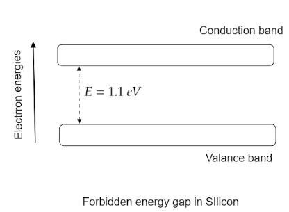
Now we have to understand what a valence band and a conduction band represent.The band in which there are available free electrons and when excited can transfer to another band is known as valence band.
Conduction band is defined as the band to which the excited electrons enter from the valence band.Silicon is considered as a semiconductor. It is used as a semiconductor in various fields.The energy gap which is the difference of energy level which an electron must surpass to transfer from the valence band to the conduction band in a Silicon is $1.1\,eV$.
Note: It must be noted that the energy gap between a metal is $0$ as the valence band and the conduction band coincide with each other. Whereas the energy gap between insulators is greater than $3{\text{ }}eV$ while in semiconductors less than $3{\text{ }}eV$.
Complete answer:
Forbidden energy gap is defined as the difference of energy from the conduction band to the valence band. In other words, it can be said that the energy that an electron requires to escape from the valence band to the conduction band is known as the forbidden energy gap.It’s SI unit is $eV$ known as electron Volt.
Now we have to understand what a valence band and a conduction band represent.The band in which there are available free electrons and when excited can transfer to another band is known as valence band.
Conduction band is defined as the band to which the excited electrons enter from the valence band.Silicon is considered as a semiconductor. It is used as a semiconductor in various fields.The energy gap which is the difference of energy level which an electron must surpass to transfer from the valence band to the conduction band in a Silicon is $1.1\,eV$.
Note: It must be noted that the energy gap between a metal is $0$ as the valence band and the conduction band coincide with each other. Whereas the energy gap between insulators is greater than $3{\text{ }}eV$ while in semiconductors less than $3{\text{ }}eV$.
Recently Updated Pages
Master Class 12 Economics: Engaging Questions & Answers for Success
Master Class 12 Physics: Engaging Questions & Answers for Success
Master Class 12 English: Engaging Questions & Answers for Success
Master Class 12 Social Science: Engaging Questions & Answers for Success
Master Class 12 Maths: Engaging Questions & Answers for Success
Master Class 12 Business Studies: Engaging Questions & Answers for Success
Trending doubts
Which are the Top 10 Largest Countries of the World?
What are the major means of transport Explain each class 12 social science CBSE
Draw a labelled sketch of the human eye class 12 physics CBSE
Why cannot DNA pass through cell membranes class 12 biology CBSE
Differentiate between insitu conservation and exsitu class 12 biology CBSE
Draw a neat and well labeled diagram of TS of ovary class 12 biology CBSE